PM851AK01 3BSE066485R1 Jumper E5 is used to configure the for redundant or non-redundant
transfer modes as well as the selection of roque master. Installing a jumper shunt on
pins 1 and 2 selects the non-redundant (fast) transfer mode. Removing (Omitting) the
jumper shunts configures the board for the redundant network transfer mode.
Installing a jumper shunt on pins 3 and 4 disables rogue master 0 function. Removing
the jumper from pins 3 and 4 enables rogue master 0 function. Installing a jumper
shunt on pins 5 and 6 disables the rogue master 1 function. Removal of the jumper
shunt on pins 5 and 6 enables the rogue master 1 function. See Table 2-2 below to
configure Jumper E5.
NOTE: The factory configuration is all jumper shunts installed, with the exception of
pins 7 and 8, which are currently not used.
Figure 2-3 Jumper E5
Table 2-2 Jumper E5 Configuration
Jumper
Position
Jumper
State Function/Mode Selected
1 and 2
Installed Non-redundant (Fast) transfer mode
Omitted Redundant transfer mode
3 and 4
Installed Rogue master 0 disabled
Omitted Rogue master 0 enabled
5 and 6
Installed Rogue master 1 disabled
Omitted Rogue master 1 enabled
7 and 8 Omitted Reserved, Not Used
Jumper E5
(Redundant Mode)
1 7 3 5
2 8 4 6
Artisan Technology Group - Quality Instrumentation ... Guaranteed | (888) 88-SOURCE | www.artisantg.com
38
2 Ultrahigh-Speed Fiber-Optic Reflective Memory with Interrupts
Registers and Memory Configuration Switches
The occupies two separate address spaces on the VMEbus (Control
and Status Register and SDRAM Memory Address spaces). The Control and Status
Register Space can be set-up for Extended Address Space (A32) or Standard Address
Space (A24) and configured to respond to either supervisory, nonprivileged or both
mode accesses.
The SDRAM Memory Space can be set-up for Extended Address Space (A32) and
configured to respond to either supervisory, nonprivileged or both mode accesses.
NOTE: It is important that the two address configurations do not overlap each other
or any other board in the system in order to work properly.
If a switch is ON, the associated Address bit is set to 0.
If a switch is OFF, the associated Address bit is set to 1.
In some cases, as in example 1, some switches are not used. If the Control and Status
Registers are configured in A24 space, switch S7 is not used, since address lines A31
through A24 are not used for A24 space.
Refer to Table 2-3 on page 41 through Table 2-5 on page 43, for examples on setting up
and configuring the register and memory switches.
NOTE: If neither Supervisory nor Nonprivileged access is enabled, the board will not
respond to any VMEbus accesses.
Artisan Technology Group - Quality Instrumentation ... Guaranteed | (888) 88-SOURCE | www.artisantg.com
39
Registers and Memory Configuration Switches 2
CSR Address Space/Access Select Switches (S7, S4 and S3)
The following switches are used to configure the Control and Status Register address
and access mode:
• S7 – Selects VMEbus addresses A32 thru A24
• S3 – Selects VMEbus addresses A23 thru A16
• S4 – Selects VMEbus addresses A15 thru A14
• S4 – Selects VMEbus access mode
Figure 2-4 Control and Status Registers VMEbus Interface Block Diagram
Hardware
Registers
VMEbus
Interface
Registers
Located in VMEbus A32, A24
Addressing Space for
Control and Status
S7 S3 S4 Off On Off On Off On
12345678
S7
Pos 1 = A24
Pos 2 = A25
Pos 3 = A26
Pos 4 = A27
Pos 5 = A28
Pos 6 = A29
Pos 7 = A30
Pos 8 = A31
S4
Pos 1 = Nonprivileged, OFF = Enabled
Pos 2 = Supervisory, OFF = Enabled
Pos 3 = Address Space A32/A24, ON = A32
Pos 4 thru 6 = Reserved (Must be OFF)
Pos 7 = A14
Pos 8 = A15
S3
Pos 1 = A23
Pos 2 = A22
Pos 3 = A21
Pos 4 = A20
Pos 5 = A19
Pos 6 = A18
Pos 7 = A17
Pos 8 = A16
Artisan Technology Group - Quality Instrumentation ... Guaranteed | (888) 88-SOURCE | www.artisantg.com
40
2 Ultrahigh-Speed Fiber-Optic Reflective Memory with Interrupts
Memory Address/Access Select Switch (S8)
Switch S8 is used to configure the SDRAM Memory address and access mode:
• S8 – Selects VMEbus addresses A32 thru A26
• S8 – Selects VMEbus access mode
Figure 2-5 SDRAM Memory VMEbus Interface Block Diagram
DRAM
A32
D32, D16, D08
BLT
SDRAM
VMEbus A32
Addressing used for
Reflective Memory data Off
On
S8
12345678 Pos 8 = A31
Pos 7 = A30
Pos 6 = A29
Pos 5 = A28
Pos 4 = A27
Pos 3 = A26
Pos 2 = Supervisory, OFF = Enabled
Pos 1 = Nonprivileged, OFF = Enabled
Extended
Artisan Technology Group - Quality Instrumentation ... Guaranteed | (888) 88-SOURCE | www.artisantg.com
41
Registers and Memory Configuration Switches 2
Example 1: Register and Memory Select
The Control and Status Registers are mapped at Standard Address $00400000 and
responds to Supervisory Mode access only.
The SDRAM reflected memory is mapped at Extended Address $80000000 and
responds to either Supervisory or Nonprivileged Mode accesses.
NOTE: It is important that the two address configurations do not overlap each other
or any other board in the system in order to work properly.
Table 2-3 Example 1. for Control and Status/Memory Switch Configuration
SW Control and Status Register
Address/Access Configuration SW SDRAM Memory Address/Access
Configuration
S7
S7 position 8 – NA (not used)
S8
S8 position 8 – OFF (A31 = 1)
S7 position 7 – NA (not used) S8 position 7 – ON (A30 = 0)
S7 position 6 – NA (not used) S8 position 6 - ON (A29 = 0)
S7 position 5 – NA (not used) S8 position 5 – ON (A28 = 0)
S7 position 4 – NA (not used) S8 position 4 – ON (A27 = 0)
S7 position 3 – NA (not used) S8 position 3 – ON (A26 = 0)
S7 position 2 – NA (not used) S8 position 2 - OFF (Supervisory Mode)
S7 position 1 – NA (not used) S8 position 1 - OFF (Nonprivileged Mode)
S3
S3 position 1 – ON (A23 = 0)
S3 position 2 – OFF (A22 = 1)
S3 position 3 – ON (A21 = 0)
S3 position 4 – ON (A20 = 0)
S3 position 5 – ON (A19 = 0)
S3 position 6 – ON (A18 = 0)
S3 position 7 – ON (A17 = 0)
S3 position 8 – ON (A16 = 0)
S4
S4 position 8 – ON (A15 = 0)
S4 position 7 – ON (A14 = 0)
S4 position 3 = OFF (A24 Space)
S4 position 2 - OFF (Supervisory Mode)
S4 position 1 - ON (Nonprivileged Mode)
Artisan Technology Group - Quality Instrumentation ... Guaranteed | (888) 88-SOURCE | www.artisantg.com
42
2 Ultrahigh-Speed Fiber-Optic Reflective Memory with Interrupts
Example 2: Register and Memory Select
The Control and Status Registers are mapped at Extended Address $30000000 and
responds to Supervisory mode access only.
The SDRAM reflected memory is mapped at Extended Address $40000000 and
responds to Nonprivileged mode access only.
NOTE: It is important that the two address configurations do not overlap each other
or interfere with the operation of any other board in the system.
Table 2-4 Example 2. for Control and Status/Memory Switch Configuration
SW Control and Status Register
Address/Access Configuration SW SDRAM Memory Address/Access
Configuration
S7
S7 position 8 – ON (A31 = 0)
S8
S8 position 8 – ON (A31 = 0)
S7 position 7 – ON (A30 = 0) S8 position 7 – OFF (A30 = 1)
S7 position 6 – OFF (A29 = 1) S8 position 6 - ON (A29 = 0)
S7 position 5 – OFF (A28 = 1) S8 position 5 – ON (A28 = 0)
S7 position 4 – ON (A27 = 0) S8 position 4 – ON (A27 = 0)
S7 position 3 – ON (A26 = 0) S8 position 3 – ON (A26 = 0)
S7 position 2 – ON (A25 = 0) S8 position 2 - ON (Supervisory Mode)
S7 position 1 – ON (A24 = 0) S8 position 1 - OFF (Nonprivileged Mode)
S3
S3 position 1 – ON (A23 = 0)
S3 position 2 – ON (A22 = 0)
S3 position 3 – ON (A21 = 0)
S3 position 4 – ON (A20 = 0)
S3 position 5 – ON (A19 = 0)
S3 position 6 – ON (A18 = 0)
S3 position 7 – ON (A17 = 0)
S3 position 8 – ON (A16 = 0)
S4
S4 position 8 – ON (A15 = 0)
S4 position 7 – ON (A14 = 0)
S4 position 3 - ON (A32 Space)
S4 position 2 - OFF (Supervisory Mode)
S4 position 1 - ON (Nonprivileged Mode)
Artisan Technology Group - Quality Instrumentation ... Guaranteed | (888) 88-SOURCE | www.artisantg.com
43
Registers and Memory Configuration Switches 2
Example 3: Register and Memory Select
The Control and Status Registers are mapped at Extended Address $70000000 and
respond to either Supervisory or Nonprivileged mode accesses.
The SDRAM reflected memory is mapped at Extended Address $78000000 and
responds to either Supervisory or Nonprivileged mode accesses.
NOTE: It is important that these two address configurations do not overlap each
other or any other board in the system in order to work properly.
Table 2-5 Example 3. for Control and Status/Memory Switch Configuration
SW Control and Status Register
Address/Access Configuration SW SDRAM Memory Address/Access
Configuration
S7
S7 position 8 – ON (A31 = 0)
S8
S8 position 8 – ON (A31 = 0)
S7 position 7 – OFF (A30 = 1) S8 position 7 – OFF (A30 = 1)
S7 position 6 – OFF (A29 = 1) S8 position 6 - OFF (A29 = 1)
S7 position 5 – OFF (A28 = 1) S8 position 5 – OFF (A28 = 1)
S7 position 4 – ON (A27 = 0) S8 position 4 – OFF (A27 = 1)
S7 position 3 – ON (A26 = 0) S8 position 3 – ON (A26 = 0)
S7 position 2 – ON (A25 = 0) S8 position 2 - OFF (Supervisory Mode)
S7 position 1 – ON (A24 = 0) S8 position 1 - OFF (Nonprivileged Mode)
S3
S3 position 1 – ON (A23 = 0)
S3 position 2 – ON (A22 = 0)
S3 position 3 – ON (A21 = 0)
S3 position 4 – ON (A20 = 0)
S3 position 5 – ON (A19 = 0)
S3 position 6 – ON (A18 = 0)
S3 position 7 – ON (A17 = 0)
S3 position 8 – ON (A16 = 0)
S4
S4 position 8 – ON (A15 = 0)
S4 position 7 – ON (A14 = 0)
S4 position 3 - ON (A32 Space)
S4 position 2 - OFF (Supervisory Mode)
S4 position 1 - OFF (Nonprivileged Mode)
Artisan Technology Group - Quality Instrumentation ... Guaranteed | (888) 88-SOURCE | www.artisantg.com
44
2 Ultrahigh-Speed Fiber-Optic Reflective Memory with Interrupts
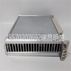
Physical Installation
CAUTION: Do not install or remove the board while power is applied.
The following procedure outlines the installation of the in a VMEbus
chassis and the set-up of the network ring topology. The can be
installed in any slot with the exception of slot one, which normally is reserved for the
system controller.
1. Before installation of the board in the chassis, ensure that all switches are set for
the desired mode of operation. Refer to Switch/Jumper Configuration and Location
on page 36.
2. With the power turned OFF, install the into the chassis, making
sure that the board connectors are firmly mated to the backplane connectors.
3. Secure the to the chassis using the two screws located at the top
and bottom of the front panel.
4. Connect the fiber-optic cables to the TX and RX connectors.
5. Route the fiber-optic cable connected to TX to the RX connector of the next board
in the ring. Connect the fiber-optic cable from that board’s TX to the RX
connector of the next board. Repeat this step until the last node in the ring routes
its TX to the RX of the first node. Refer to Figure 2-9 on page 47 for an example of
a six node ring.
Figure 2-6 Typical Installation Using the and VMIPCI-5565
VMIC's
UltraHigh-Performance
Reflective Memory
Board
Multimode or Single Mode
Fiber-Optic Cable
VMEbus
Chassis (Available from VMIC)
VMIVME
VMIVME
5565
5565
VMIPCI-5565
Standard P.C.
System with a
VMIPCI-5565 (available
from VMIC)
Installed
Artisan Technology Group - Quality Instrumentation ... Guaranteed | (888) 88-SOURCE | www.artisantg.com
45
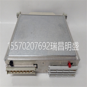
Front Panel Description 2
Front Panel Description
The has an optical transceiver located on the front panel. Figure 2-7
below is an illustration of the front panel. The Reflective Memory board has three LED
indicators located on the front panel. Table 2-6 below outlines the front panel LEDs.
The port labeled “RX” is the receiver and the port labeled “TX” is the transmitter. The
uses “LC” type fiber-optic cables either single-mode or multimode.
CAUTION: When the fiber-optic cables are not connected, install the supplied dust
caps to keep dust and dirt out of the optics. Do not power up the
without the fiber-optic cables installed. To avoid potential eye injuries, do not look
directly into the transmitters when power is applied.
Figure 2-7 Front Panel
The status LEDs power up default state is “ON”. The LED is a user defined board
status indicator. The status LED can be toggled “ON” or “OFF” by writing to Bit 31 of
the Control and Status register. The signal detect LED turns “ON” if the receiver
detects light and it can be used as a simple method of verifying the optical network is
properly connected to the receiver. The Own Data LED is turned “ON” when the
board detects its own data returning over the network.
Table 2-6 LED Descriptions
LED Color Description
Own Data Green Detects when own data is received.
SIG. DET. Yellow Indicates optical network connection.
Status Red User defined board status indicator.
TX
RX
OWN DATA
SIG. DET.
STATUS
VMEbus
VMIVME
5565
Artisan Technology Group - Quality Instrumentation ... Guaranteed | (888) 88-SOURCE | www.artisantg.com
46
2 Ultrahigh-Speed Fiber-Optic Reflective Memory with Interrupts
Cable Configuration
The is available with a multimode or single-mode fiber-optic interface.
Figure 2-8 is an illustration of the ‘LC’ type multimode or single-mode fiber-optic
cable connector.
Cable Specification:
• Simplex, multimode, graded index glass fiber
• Core diameter = 62.5 ±3 µm
• Cladding diameter = 125 ±2 µm
• Jacket outer diameter = 3.0 mm ±.1mm
• Attenuation: 4.0 dB/km (max) at 850nm, 1.75dB/km (max) at 1300nm
• Bandwidth: 160 to 300 MHz-Km (min) at 850 nm, 300 to 700 MHz-km (min) at
1300 nm
• UL type OFNR, CSA type OFN FT4
Connector Specification:
• Compatible with NTT LC standard and JIS C 5973 compliant
• Ceramic ferrule
• Insertion loss: 0.35 dB (max) multimode
• Fiber clad diameter: 125 µm
• Jacket diameter: 3.0 mm
• Temperature range: -20 °C to +85 °C
Figure 2-8 ‘LC’ Type Multimode Fiber-Optic Cable Connector
0.84 (21.23)
0.49
(1.25)
Dimensions: inches (mm)
(2.9mm)
Artisan Technology Group - Quality Instrumentation ... Guaranteed | (888) 88-SOURCE | www.artisantg.com
47
Connectivity 2
Connectivity
Figure 2-9 Example: Six Node Ring Connectivitybase. The base address is
determined using switches S7, S4 and S3.
Reflective Memory (RFM) Control and Status Registers – The RFM Control and
Status Registers implement the functions unique to the VMIxxx-5565 Reflective
Memory board. These functions include RFM operation status, detailed control of the
RFM sources for the VMEbus interrupt, and network interrupt access. These registers
are located at $1200 offset from base. The base address is determined using switches
S7, S4 and S3.
Artisan Technology Group - Quality Instrumentation ... Guaranteed | (888) 88-SOURCE | www.artisantg.com
24
1 Ultrahigh-Speed Fiber-Optic Reflective Memory with Interrupts
Reflective Memory RAM
The actual on-board Reflective Memory SDRAM is available in two sizes: 64 Mbytes
or 128 Mbytes with parity. The SDRAM starts at the location specified by switch S8.
Unlike the previous versions of VMIC’s Reflective Memory products, the RFM
Control and Status Registers do NOT replace the first $40 locations of RAM.
Parity Function
The parity function is not enabled at power up and must be enabled by setting Bit 13
in the RFM CSR’s Local Interrupt Enable (LIER) register at offset $14. To use the parity
function, writes must occur on 32-bit (Lword) or 64-bit (Qword) boundaries. While
parity is active, 8-bit (byte) writes and 16-bit (word) writes are prohibited. In addition,
since the RAM does not power up in a valid parity state, any location that is to be read
with parity must first be initialized by a write of some data pattern. Otherwise the
read will assert an erroneous parity error.
Artisan Technology Group - Quality Instrumentation ... Guaranteed | (888) 88-SOURCE | www.artisantg.com
25
Interrupt Circuits 1
Interrupt Circuits
The has a single programmable VMEbus interrupt output. One or
more events on the can cause the interrupt. The sources of the
VMEbus interrupt can be individually enabled and monitored through several
registers.
The interrupts are selected and monitored through the two RFM CSRs
referred to as the Local Interrupt Status Register (LISR) and the Local Interrupt Enable
Register (LIER). For a detailed description of the two registers refer to the
Programming section. A block diagram of the main interrupt circuitry is shown in
Figure 1-1 on page 26.
Artisan Technology Group - Quality Instrumentation ... Guaranteed | (888) 88-SOURCE | www.artisantg.com
26
1 Ultrahigh-Speed Fiber-Optic Reflective Memory with Interrupts
Figure 1-1 Interrupt Circuitry Block Diagram
Network
Receiver
Circuitry
Network
Interrupt FIFO's
4
Local Interrupt Status Register (LISR)
(Offset $10)
Local Interrupt Enable Register (LIER)
(Offset $14)
RFM Control and Status Registers
RFM
Fault/Status
Events
+
LINT0
VMEbus Interrupt Enable Register (VINT_EN)
(Offset $310)
Bit 0
DMA
Bit 08
Universe II Registers
VMEbus Interrupts (1 thru 7)
Artisan Technology Group - Quality Instrumentation ... Guaranteed | (888) 88-SOURCE | www.artisantg.com
27
Interrupt Circuits 1
Network Interrupts
The has the capability of passing interrupt packets over the network in
addition to data. The network interrupt packets can be directed to a specific node or
broadcast globally to all nodes on the network. Each network interrupt packet
contains the sender’s node ID, the target (destination) node ID, the interrupt type
information and 32 bits of user defined data.
The types of network interrupts include four (4) general purpose interrupts. The
sending node specifies the target (destination) node, the interrupt type and 32 bits of
data using three RFM Control and Status registers. Each receiving node evaluates the
interrupt packets as they pass through. If the interrupt is directed to that node, then
the sender’s node ID is stored in the appropriate Sender ID FIFO (one of four). The
Sender ID FIFO is 127 locations deep. The data will be stored in a companion 127
locations deep data FIFO.
If enabled through the LISR, LIER and VINT_EN registers, any of the four possible
network interrupts can also generate a host VMEbus interrupt at each receiving node.
Artisan Technology Group - Quality Instrumentation ... Guaranteed | (888) 88-SOURCE | www.artisantg.com
28
1 Ultrahigh-Speed Fiber-Optic Reflective Memory with Interrupts
Redundant Transfer Mode of Operation
The is capable of operating in a Redundant Transfer mode. The board
is configured for redundant mode when pins 1 and 2 of jumper E5 has the shunt
removed. While in the redundant transfer mode, each packet will be transferred
twice, regardless of the dynamic packet size. The receiving node evaluates each of the
redundant transfers. If no errors are detected in the first transfer, it is used to update
the on-board memory and the second transfer is discarded. If however the first
transfer does contain an error, the second transfer is used to update the on-board
memory provided it has no transmission errors. If errors are detected in both
transfers, the transfers will not be used and the data is completely removed from the
network. The Bad Data bit (Bit 01 of the LCSR) will be set if an error is detected in
either transfer.
Redundant transfer mode greatly reduces the chance that any data is dropped from
the network. However, the redundant transfer mode also reduces the effective
network transfer rates. The single Lword (4 byte) transfer rate drops from the
non-redundant rate of 43 Mbyte/sec. to approximately 20 Mbytes/sec. The 16 Lword
(64 byte) transfer rate drops from the non-redundant rate of 174 Mbyte/sec. to the
redundant rate of 87 Mbyte/sec.
Rogue Packet Remove Operation
A rogue packet is a packet that does not belong to any node on the network. Recalling
the basic operation of Reflective Memory, one node originates a packet on the
network in response to a memory write from the host. The packet is transferred
around the network to all nodes until it returns to the originating node. It is then a
requirement of the originating node to remove the packet from the network. If,
however, the packet somehow gets altered as it passes through another node or if the
originating node begins to malfunction, then the originating node may fail to
recognize the packet as its own and will not remove the packet from the network. In
this case the packet will continue to pass around the network.
Rogue packets are extremely rare. Their existence indicates a malfunctioning board
due to true component failure or due to operation in an harsh environment. Normally,
the solution is to isolate and replace the malfunctioning board and/or improve the
environment. However, some users prefer to tolerate sporadic rogue packets rather
than halt the system for maintenance provided the rogue packets are removed from
the network.
To provide tolerance to rogue packet faults, the can operate as one of
two rogue masters. A rogue master alters each packet as it passes from one node to
another. When the packet returns to the rogue master a second time, the rogue master
recognizes that it is a rogue packet and removes it from the ring. When a rogue packet
is detected, a rogue packet fault flag is set in the Local Interrupt Status Register (LISR).
The assertion of the rogue packet fault bit may optionally assert a VMEbus interrupt
to inform the host that the condition exists.
Rogue Master 0 and Rogue Master 1, are provided to cross check each other. Rogue
Master 0 is enable removing the jumper shunt from E5 pins 3 and 4. Rogue Master 1 is
enable by removing the jumper shunt from E5 pins 5 and 6. See “
Location of User Configurable Switches and Jumpers” on page 35.
NOTE: Two boards in the network should not be set as the same rogue master.
Otherwise, one of the two will erroneously remove packets originated by the other.
Artisan Technology Group - Quality Instrumentation ... Guaranteed | (888) 88-SOURCE | www.artisantg.com
29
Byte Ordering: Big Endian / Little Endian 1
Byte Ordering: Big Endian / Little Endian
The byte-ordering issue exists due to the different traditions at the major
microprocessor manufacturers, Motorola and Intel. VMEbus boards are designed
around Motorola’s 680X0 processors and compatibles, which store multiple-byte
values in memory with the most significant byte at the lowest byte address. This
byte-ordering scheme became known as “Big Endian” ordering. On the other hand,
Intel’s 80X86 microprocessors, store multiple-byte values in memory with the least
significant byte in the lowest byte address, earning the name “Little Endian” ordering.
The ’s PCI-to-VMEbus interface uses an Intel based or equivalent
bridge chip, which uses Little Endian byte ordering. Byte arrangement and the byte
relationship between data in the processor and transferred data in memory are shown
in Figure 1-2.
Figure 1-2 Byte Relationships Using the Little Endian Pentium Microprocessor
Note that in Little Endian devices, the Memory’s least significant byte is stored in the
lowest byte address after a multiple-byte write (such as the Lword transfer
illustrated), while the Reflective Memory’s most significant byte is stored in the
highest byte address after such transfers. Conversely, the processor considers data
retrieved from the lowest byte address to be the least significant byte after a
multiple-byte read. Data retrieved from the highest byte address is considered to be
the most significant byte.
Contrast the behavior of the Little Endian Pentium in Figure 1-2 with the same Lword
transfer using a Big Endian processor like the Motorola 68040 in Figure 1-3 on
page 30.
Note that the Big Endian 68040 handles the same Lword transfer in a completely
different manner than the Little Endian Pentium microprocessor. During a
multiple-byte transfer like the Lword transfer illustrated, a Big Endian processor
writes its least significant byte in the highest byte address in memory, while its most
significant byte is written to the lowest address. The converse is true during read
operations: the data in the lowest byte address is considered to be the most significant,
while the byte in the highest address is considered to be the least significant.
D31-D24 D23-D16 D15-D08 D07-D00
MSB LSB
Data Within the Pentium Microprocessor
BYTE $03
BYTE $02
BYTE $01
BYTE $00
.
.
.
Data Within
Memory
Lword (32-bit) Transfer
MSB
LSB
Artisan Technology Group - Quality Instrumentation ... Guaranteed | (888) 88-SOURCE | www.artisantg.com
30
1 Ultrahigh-Speed Fiber-Optic Reflective Memory with Interrupts
Figure 1-3 Byte Relationships Using the Big Endian 68040 Microprocessor
The VMEbus Specification does not specify which byte of a multiple-byte transfer is
most significant. The VMEbus Specification does, however, require certain byte lanes
to be associated with certain byte addresses. As shown in Table 1-1 on page 31, byte(0)
must be transferred on data lines D31-D24 during a Lword transfer while byte(3)
must be transferred on lines D7-D0. This byte and address alignment is exactly the
same as that for a Big Endian processor such as the Motorola 68040.
If a Little Endian device were to have its data bus directly connected to the VMEbus
(i.e., D31 to D31, D30 to D30, etc.), then the most significant byte data supplied to the
VMEbus D31-D24 byte lane during a Lword write would be stored by the VMEbus in
the lowest of the four destination byte addresses – opposite that expected by the
Pentium microprocessor. This poses no problem if the 32-bit value written is always
read back using a similar Lword transfer (i.e., all four bytes at once), since the
swapped data gets swapped again and appears to the Host exactly as it should.
However, if the data written by the 32-bit Lword transfer were to be retrieved using
any other method, for example, using four separate byte transfers creates a problem.
The data at the lowest byte address would be incorrectly assumed to be the least
significant, while it is actually the most significant.
The problem cannot be solved by simply connecting the to the
VMEbus with its byte lanes crossed. For example, the uses D0-D7 to
transfer a byte to address $00, while the VMEbus requires D8-D15 be used. For this
reason, special hardware has been incorporated into the
PCI-to-VMEbus interface to facilitate different kinds of byte swapping for varying
circumstances.
D31-D24 D23-D16 D15-D08 D07-D00
MSB LSB
Data Within the 68040 Microprocessor
BYTE $03
BYTE $02
BYTE $01
BYTE $00
.
.
.
DataWithin
Memory
Lword (32-bit) Transfer
MSB
LSB
Artisan Technology Group - Quality Instrumentation ... Guaranteed | (888) 88-SOURCE | www.artisantg.com
31
Byte Ordering: Big Endian / Little Endian 1
Endian Conversion Hardware
The Universe II chip performs Address Invariant translation between the PCI and
VMEbus interfaces. Address Invariant mapping or “Non-endian conversion” mode
maintains the byte ordering between the two interfaces (i.e. data originating in
Little Endian mode on the PCI side will remain in Little Endian mode on the VMEbus
side of the interface). However, the PCI-to-VMEbus interface has
external endian conversion logic which allows the applicati |