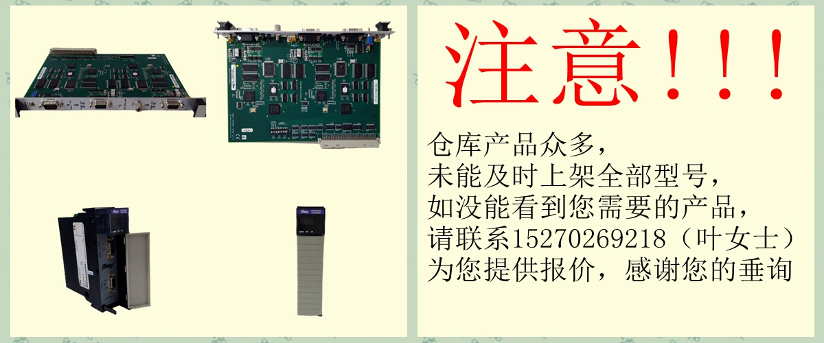


atIS220UCSAH1AK
数据和电源的链接。这个
数据链路是同步的,并监控差异。金融情报室和情报室都有飞机
用于表征温度相关问题的温度传感器。
HIU和FIU板的电源都是冗余的、完全仪表化的,并且
这是可测试的。这些组件一起构成电源完整性子系统。
1.8.事件序列特征
该模块自动测量磁场电压和电流,以确定磁场状态
每个输出通道。当输出从一种状态转换到另一种状态时,会发生事件
另一个当信道改变状态时,会记录车载定时器值。当
TMR处理器接下来从输出模块读取数据、信道状态和实时数据
检索时钟值。TMR处理器使用该数据将状态变化记录到
系统事件序列(SOE)日志。用户可以将每个输出配置为包括在
系统SOE日志。SOE的完整详细信息包含在可信的事件序列和
过程历史记录软件包,发表于ICSTT-RM243(PD-T8013)。
1.说明:可信TMR 24Vdc数字输出模块–40信道
814期罗克韦尔自动化出版物ICSTT-RM280N-EN-P
1.9.输出开关结构
数字输出模块提供了一种TMR开关拓扑,其中负载由电源驱动
总共三个完全监控的故障安全(6个元件)开关通道,一个物理驻留
在模块中的每个FIU上。任何单个开关或整个片故障都会留下两个
在为负载供电的三个故障安全开关通道中。
图3输出开关结构
图3中所示的上部开关表示为N.O.(常开),并且为:
由他们实际居住的金融情报室控制。1.下部开关为:
其被描述为N.C.(常闭),并由相邻的FIU.2的“上游”控制
注:在这种情况下,N.O.定义为在没有控制信号电源的情况下处于关闭状态,以及
类似地,N.C.是在没有控制信号功率的情况下的导通状态。这些交换机由以下部件构成:
增强型MOSFET和均保证在没有模块电源的情况下关闭,以创建
栅极电压信号将其偏置到3(例如,与机电继电器不同)。
在没有控制信号的情况下,下开关被指定为接通的原因
电源允许两个通道在整个片发生故障时为负载供电。即使整个系统
片故障时,幸存的输出电路将承载NECE
IS220UCSAH1AK
IS220UCSAH1AK
ed links for data and power. The data link is synchronized and monitored for variance. Both FIU and HIU have on-board temperature sensors to characterize temperature-related problems. The power supplies for both the HIU and FIU boards are redundant, fully instrumented and testable. Together these assemblies form a Power Integrity Sub-system. 1.8. Sequence of Events Characteristics The Module automatically measures the field voltage and current to determine the state of each output channel. An event occurs when the output transitions from one state to another. When a channel changes state, the on-board timer value is recorded. When the TMR Processor next reads data from the Output Module, the channel state and real-time clock value are retrieved. The TMR Processor uses this data to log the state change into the system Sequence of Events (SOE) log. The user may configure each output to be included in the system SOE log. Full details of SOE are contained in Trusted Sequence of Events and Process Historian Package, publication ICSTT-RM243 (PD-T8013). 1. Description Trusted TMR 24Vdc Digital Output Module – 40 Channel 8 Issue 14 Rockwell Automation Publication ICSTT-RM280N-EN-P 1.9. Output Switch Structure The Digital Output Module provides a TMR switch topology where the load is driven by a total of three fully monitored, fail safe (6 element) switch channels, one physically resident on each FIU in the Module. Any single switch or entire slice failure is designed to leave two of the three fail safe switch channels operational to power the load. Figure 3 Output Switch Structure The upper switches as shown in Figure 3 are denoted as N.O. (Normally Open), and are controlled by the FIU on which they are physically resident.1 The lower switches are depicted as N.C. (Normally Closed), and are controlled by the “upstream” neighbouring FIU.2 Note: In this context, N.O. is defined as being in the off state in the absence of control signal power, and similarly, N.C. is the on state in the absence of control signal power. These switches are constructed from enhancement mode MOSFETs and are both guaranteed to be off in the absence of Module power to create gate voltage signals to bias them on3 (unlike electromechanical relays for example). The reason that the lower switches are specified to be on in the absence of control signal power is to allow two channels to power the load should an entire slice fail. Even if an entire slice fails, the surviving output circuits will carry the neces
Copyright ©2019-2022 瑞昌明盛自动化设备有限公司 版权所有 赣ICP备2021006016号