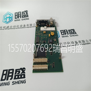
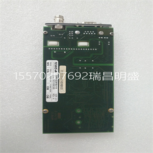
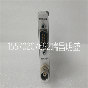
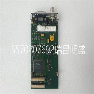


TEWS TPMC815-11
TPMC815使用SMSC的COM20020 ARCNET控制器。
可使用PCI9030 PCI的本地空间在PCI空间中访问COM20020寄存器
目标芯片。
完整的TPMC815 ARCNET接口由COM20020 ARCNET控制器控制。
有关详细的功能说明,请参阅COM20020数据表。
TPMC815还提供一个8 x dip开关。软件可使用dip开关设置进行以下操作:
对COM20020节点ID寄存器进行编程。
TPMC815用户手册版本2.0.29页,共20页
4局部空间寻址
4.1 PCI9030局部空间配置
通过使用PCI9030本地总线从PCI侧访问本地板载可寻址区域
空间。
PCI9030
地方的
空间
PCI9030
PCI基址
(PCI中的偏移量)
配置
空间)
PCI
空间
映射
大小
(字节)
港口城市
宽度
(比特)
字节序
模式
描述
0 2(0x18)IO 16 8点亮本地寄存器
空间
1 3(0x1C)内存256 8点亮本地寄存器
空间
2.4(0x20)---未使用
3.5(0x24)---未使用
表4-1:PCI9030本地空间配置
TPMC815用户手册版本2.0.210页,共20页
4.2本地寄存器空间地址映射
PCI基址=
PCI I/O空间映射:
PCI9030 PCI基址2(PCI9030PCI配置空间中的偏移量0x18)
PCI内存空间映射:
PCI9030 PCI基址3(PCI9030PCI配置空间中的偏移量0x1C)
偏移到PCI
基址
注册名称和大小
(比特)
COM20020寄存器
0x00状态/中断掩码8
0x01诊断状态/命令8
0x02地址指针高8
0x03地址指针低8
0x04数据8
0x05子地址8
0x06配置8
0x07暂定ID 8
节点ID
设置1
下一个ID/测试
设置2
附加寄存器
0x08 ID开关8
表4-2:本地寄存器空间
4.2.1 COM20020寄存器
有关COM20020 ARCNET的详细说明,请参阅COM20020数据表
控制器寄存器。
TPMC815用户手册版本2.0.211页,共20页
4.2.2 ID开关寄存器
ID开关寄存器是一个8位只读寄存器,表示板上设备的实际设置
8个dip开关。
位开关号访问位值
7(msb)8
R
开关位置开=位值“0”
断开位置=位值“1”
6 7
5 6
4 5
3 4
2 3
1 2
0(lsb)1
表4-3:ID开关寄存器
软件可以读取ID开关寄存器以编程COM20020节点ID寄存器。
TPMC815用户手册版本2.0.212页,共20页
5 PCI9030目标芯片
5.1 PCI配置寄存器(PCR)
5.1.1 PCI9030 PCI头
PCI-CFG
登记
住址
将“0”写入所有未使用(保留)位PCI
可写
初始值
(十六进制值)
31 24 23 16 15 8 7 0
0x00设备ID供应商ID N 032F 1498
0x04状态命令Y 0280 0000
0x08类别代码修订ID N 028000 00
0x0C BIST头类型延迟定时器缓存线大小Y[7:0]00
内存映射配置的0x10 PCI基址0。寄存器Y FFFFFF80
I/O映射配置的0x14 PCI基址1。寄存器Y FFFFFF81
0x18本地地址空间0的PCI基址2 Y FFF 1
0x1C本地地址空间1的PCI基址3 Y FFFF 00
0x20本地地址空间2 Y 00000000的PCI基址4
0x24本地地址空间3 Y 00000000的PCI基址5
0x28 PCI CardBus信息结构指针N 00000000
0x2C子系统ID子系统供应商ID N s.b.1498
0x30本地扩展ROM的PCI基址Y 00000000
0x34保留为新帽。Ptr。N 00000040
0x38保留N 00000000
0x3C Max_Lat Min_Gnt中断引脚中断线Y[7:0]00
0x40下午上限。PM Nxt。帽子下午帽。识别号:4801 48 01
0x44下午数据下午CSR分机下午CSR Y 00 0000
0x48保留为HS CSR和HS Nxt。帽子HS帽。ID Y[23:16]00 00 4C 06
0x4C VPD地址VPD Nxt。帽子VPD帽。ID Y[31:16]0000 00 03
0x50 VPD数据Y 00000000
表5-1:PCI9030 PCI头
子系统ID:TPMC815-21R:0x0015
TPMC815用户手册版本2.0.213页,共20页
5.1.2 PCI基址初始化
PCI基址初始化是PCI主机软件的范围。
PCI9030 PCI基址初始化:
1.将0xFFFF_ FFFF写入PCI9030 PCI基址寄存器。
2.读回PCI9030 PCI基址寄存器。
3.对于PCI基址寄存器0:5,检查PCI地址空间的位0:
位0='0'需要PCI内存空间映射
位0='1'需要PCI I/O空间映射
对于PCI扩展ROM基址寄存器,检查位0的使用情况:
位0='0':未使用扩展ROM
位0='1':使用扩展ROM
4.对于PCI I/O空间映射,从位位置2开始,一个位集确定
所需的PCI I/O空间大小。
对于PCI内存空间映射,从位位置4开始,设置为“1”的一位确定大小
所需的PCI存储器空间大小。
对于PCI扩展ROM映射,从位位置11开始,设置为“1”的一位确定
所需的PCI扩展ROM大小。
例如,如果PCI基址寄存器的5位被检测为设置为“1”的一位,则
PCI9030正在请求32字节的空间(地址位4:0不是基址解码的一部分)。
5.确定基址并将基址写入PCI9030 PCI B
TEWS TPMC815-11

TEWS TPMC815-11
The TPMC815 uses the COM20020 ARCNET Controller from SMSC. The COM20020 registers are accessible in PCI Space using the local spaces of the PCI9030 PCI Target Chip. The complete TPMC815 ARCNET interface is controlled by the COM20020 ARCNET Controller. Please refer to the COM20020 data sheet for a detailed functional description. The TPMC815 also provides an 8 x dip-switch. Software may use the dip-switch setting for programming the COM20020 Node-ID Register. TPMC815 User Manual Issue 2.0.2 Page 9 of 20 4 Local Space Addressing 4.1 PCI9030 Local Space Configuration The local on board addressable regions are accessed from the PCI side by using the PCI9030 local spaces. PCI9030 Local Space PCI9030 PCI Base Address (Offset in PCI Configuration Space) PCI Space Mapping Size (Byte) Port Width (Bit) Endian Mode Description 0 2 (0x18) IO 16 8 LIT Local Register Space 1 3 (0x1C) MEM 256 8 LIT Local Register Space 2 4 (0x20) - - - - Not Used 3 5 (0x24) - - - - Not Used Table 4-1 : PCI9030 Local Space Configuration TPMC815 User Manual Issue 2.0.2 Page 10 of 20 4.2 Local Register Space Address Map PCI Base Address = PCI I/O Space Mapped: PCI9030 PCI Base Address 2 (Offset 0x18 in PCI9030 PCI Configuration Space) PCI MEM Space Mapped: PCI9030 PCI Base Address 3 (Offset 0x1C in PCI9030 PCI Configuration Space) Offset to PCI Base Address Register Name Size (Bit) COM20020 Registers 0x00 Status / Interrupt Mask 8 0x01 Diagnostic Status / Command 8 0x02 Address Pointer High 8 0x03 Address Pointer Low 8 0x04 Data 8 0x05 Sub Address 8 0x06 Configuration 8 0x07 Tentative ID 8 Node ID Setup 1 Next ID / Test Setup 2 Additional Registers 0x08 ID Switch 8 Table 4-2 : Local Register Space 4.2.1 COM20020 Registers Please refer to the COM20020 datasheet for a detailed description of the COM20020 ARCNET Controller registers. TPMC815 User Manual Issue 2.0.2 Page 11 of 20 4.2.2 ID Switch Register The ID Switch Register is an 8 bit read only register representing the actual setting of the on board 8 x dip-switches. Bit Switch No. Access Bit Value 7 (msb) 8 R Switch Position ON = Bit value '0' Switch Position OFF = Bit value '1' 6 7 5 6 4 5 3 4 2 3 1 2 0 (lsb) 1 Table 4-3 : ID Switch Register Software may read the ID Switch Register to program the COM20020 Node-ID Register. TPMC815 User Manual Issue 2.0.2 Page 12 of 20 5 PCI9030 Target Chip 5.1 PCI Configuration Registers (PCR) 5.1.1 PCI9030 PCI Header PCI CFG Register Address Write ‘0’ to all unused (Reserved) bits PCI writeable Initial Values (Hex Values) 31 24 23 16 15 8 7 0 0x00 Device ID Vendor ID N 032F 1498 0x04 Status Command Y 0280 0000 0x08 Class Code Revision ID N 028000 00 0x0C BIST Header Type Latency Timer Cacheline Size Y[7:0] 00 00 00 00 0x10 PCI Base Address 0 for MEM Mapped Config. Registers Y FFFFFF80 0x14 PCI Base Address 1 for I/O Mapped Config. Registers Y FFFFFF81 0x18 PCI Base Address 2 for Local Address Space 0 Y FFFFFFF1 0x1C PCI Base Address 3 for Local Address Space 1 Y FFFFFF00 0x20 PCI Base Address 4 for Local Address Space 2 Y 00000000 0x24 PCI Base Address 5 for Local Address Space 3 Y 00000000 0x28 PCI CardBus Information Structure Pointer N 00000000 0x2C Subsystem ID Subsystem Vendor ID N s.b. 1498 0x30 PCI Base Address for Local Expansion ROM Y 00000000 0x34 Reserved New Cap. Ptr. N 000000 40 0x38 Reserved N 00000000 0x3C Max_Lat Min_Gnt Interrupt Pin Interrupt Line Y[7:0] 00 00 01 00 0x40 PM Cap. PM Nxt. Cap. PM Cap. ID N 4801 48 01 0x44 PM Data PM CSR EXT PM CSR Y 00 00 0000 0x48 Reserved HS CSR HS Nxt. Cap. HS Cap. ID Y[23:16] 00 00 4C 06 0x4C VPD Address VPD Nxt. Cap. VPD Cap. ID Y[31:16] 0000 00 03 0x50 VPD Data Y 00000000 Table 5-1 : PCI9030 PCI Header Subsystem-ID: TPMC815-21R: 0x0015 TPMC815 User Manual Issue 2.0.2 Page 13 of 20 5.1.2 PCI Base Address Initialization PCI Base Address Initialization is scope of the PCI host software. PCI9030 PCI Base Address Initialization: 1. Write 0xFFFF_FFFF to the PCI9030 PCI Base Address Register. 2. Read back the PCI9030 PCI Base Address Register. 3. For PCI Base Address Registers 0:5, check bit 0 for PCI Address Space: Bit 0 = '0' requires PCI Memory Space mapping Bit 0 = '1' requires PCI I/O Space mapping For the PCI Expansion ROM Base Address Register, check bit 0 for usage: Bit 0 = ‘0’: Expansion ROM not used Bit 0 = ‘1’: Expansion ROM used 4. For PCI I/O Space mapping, starting at bit location 2, the first bit set determines the size of the required PCI I/O space size. For PCI Memory Space mapping, starting at bit location 4, the first bit set to '1' determines the size of the required PCI Memory space size. For PCI Expansion ROM mapping, starting at bit location 11, the first bit set to '1' determines the required PCI Expansion ROM size. For example, if bit 5 of a PCI Base Address Register is detected as the first bit set to ‘1’, the PCI9030 is requesting a 32 byte space (address bits 4:0 are not part of base address decoding). 5. Determine the base address and write the base address to the PCI9030 PCI Base Address Register. For PCI Memory Space mapping the mapped address region must comply with the definition of bits 3:1 of the PCI9030 PCI
Copyright ©2019-2022 瑞昌明盛自动化设备有限公司 版权所有 赣ICP备2021006016号