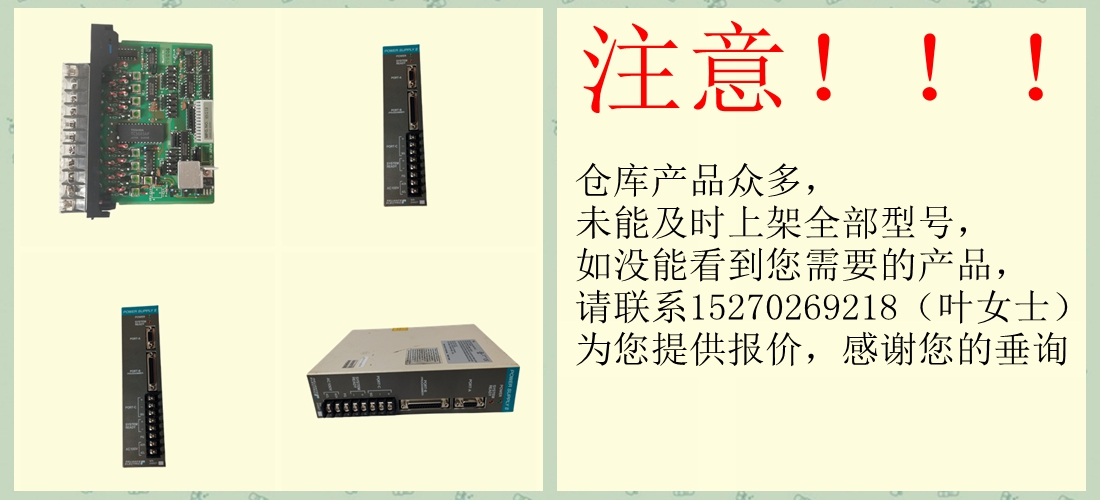


1C31113G03
7.18~F7.25预留
F7.26终端AO1的功能范围:0~11【0】
F7.27终端AO2的功能范围:0~11【3】
F7.28终端DO范围的功能:0~11【0】
AO1和AO2是模拟输出端子,DO是
脉冲输出端子。
有关输出特性,请参阅第3.3.2节
AO1和AO2,其模拟输出范围由下式定义:
F7.29。
DO的脉冲频率范围:0~大输出脉冲
频率(由F7.32定义)。
显示范围和
表中给出了AO1、AO2和DO的输出值
5-12.
表5-12输出端子显示范围
设置功能范围
0
输出频率
滑前
补偿
0~大输出
频率
1输出频率后
滑差补偿
0~大输出
频率
2.预设频率0~大输出
频率
3.输出电流:驱动器的0~2倍
额定电流
4.输出电流:电机的0~2倍
额定电流
5.输出转矩:电机的0~2倍
额定转矩
6.输出电压:驱动器的0~1.2倍
额定电压
7母线电压0~800V
8 VCI 0~10V
设置功能范围
9 CCI 0~10V/0~20mA
10输出功率:0~2倍额定值
权力
11扩展功能
主机2 0~65535
如果主机2的扩展功能2已启用,则
端子Y1、Y2或TC的输出信号直接为
由串行端口控制。“65535”对应于
大输出为10V(或20mA)。参考
有关详细信息,请参阅EV2000的通信协议。
例如:
AO1输出4~20mA,表示母线电压
0~800V。
设置:
①F7.26=7,输出母线电压;
②F7.29=01,端子AO1的输出为4~20mA;
③F7.30=100%,输出增益为100%;
④CN16的AO1跳线在0/4-20mA侧短路。
注:
如果端子X8选择44~46的功能,则DO被禁用
自动地
F7.29模拟输出范围
选择范围:00~11【00】
A、B、C、D
AO1输出范围
0:0~10V或0~20mA
1: 2~10V或4~20mA
保留
AO2输出范围
0:0~10V或0~20mA
1: 2~10V或4~20mA
保留
图5-49模拟输出偏移设置
哪里
A: 千人之地B:百人之地
C: 十位D:单位位
F7.29用于选择AO1和
AO2。
F7.30 AO1范围的输出增益:0.0~200.0%
【100.0%】
F7.31 AO2范围的输出增益:0.0~200.0%
【100.0%】
68第5章参数介绍
EV2000系列通用变速驱动用户手册
对于AO1和AO2的模拟输出,您可以调整
改变测量范围的输出增益,或
校准仪表。
注:
更改F7.30和F7.31的设置将影响
模拟输出。
F7.32大输出
DO频率
范围:0~50.0kHz
【10.0KHz】
F7.32定义了允许的大频率:
请参见F7.28。
F7.33预设计数值范围:F7.34~9999【0】
F7.34指定计数值范围:0~F7.33【0】
F7.33和F7.34是对12号和13号的补充
表5-11中的功能。
定义了Xi接收到脉冲F7.33个数后,
继电器或Yi(双向集电极开路输出
终端)将给出信号。
例如:如图5-50所示,当第八
脉冲信号由端子Xi接收,Y1输出
指示信号。此时F7.33=8。
当Xi收到F7.34的脉冲数时,易就会发出
信号将持续到F7.33到达。
如图5-50所示,当Xi接收到第5个脉冲时,
Y2输出指示信号。直到X1收到
第八脉冲。在这种情况下,F7.34=5,F7-33=8。F7-34为
如果大于F7.33,则无效。
Xi 1 2 3 4 5 67 89
输入
Y1
Y2
图5-50预设和指定脉冲数
F7.35端子正极和
否定逻辑
范围:000~FFFH
【000H】
A、B、C、D
BIT0:X1的正/负逻辑
BIT1:X2的正/负逻辑
BIT2:X3的正/负逻辑
BIT3:X4的正/负逻辑
BIT0:X5的正/负逻辑
BIT1:X6的正/负逻辑
BIT2:X7的正/负逻辑
BIT3:X8的正/负逻辑
BIT0:FWD的正/负逻辑
BIT1:版本的正/负逻辑
BIT2:Y1的正/负逻辑
BIT3:Y2的正/负逻辑
BIT0:保留
BIT1:保留
BIT2:保留
BIT3:保留
图5-51端子正负逻辑
哪里
A: 千人之地B:百人之地
C: 十位D:单位位
F7.35定义了终端的正逻辑和负逻辑
正向逻辑:如果端子Xi连接到
公共终端;
负逻辑:如果端子Xi连接,则其被禁用
连接到公共终端;
如果该位设置为0,则表示正逻辑;如果设置为1,则
这意味着否定逻辑。
例如:
如果要求X1~X8为正逻辑,则端子
FWD和REV需要为负逻辑,
端子Y1为正逻辑,端子Y2为负逻辑
逻辑,然后设置:
X4~X1的逻辑状态为0000,十六进制值为0;
X8~X5的逻辑状态为0000,十六进制值为0,;
Y2、Y1、REV和FWD的逻辑状态为1011,并且
十六进制值为B,因此F7.35应设置为“0B00”。参考
见表5-13。
表5-13二进制代码和十六进制值的转换
二进制设置
比特3比特2比特1
1C31113G03
1C31113G03
7.18~F7.25 Reserved
F7.26 Functions of terminal AO1 Range:0~11【0】
F7.27 Functions of terminal AO2 Range:0~11【3】
F7.28 Functions of terminal DO Range:0~11【0】
AO1 and AO2 are analog output terminals, and DO is
pulse output terminals.
Refer to section 3.3.2 for the output characteristics of
AO1 and AO2, their analog output ranges are defined by
F7.29.
Pulse frequency range of DO: 0~Max output pulse
frequency (defined by F7.32).
The relationship between the displaying range and the
output values of AO1, AO2 and DO are given in Table
5-12.
Table 5-12 Displaying range of output terminals
Setting Functions Range
0
Output frequency
before slip
compensation
0~Max output
frequency
1 Output frequency after
slip compensation
0~Max output
frequency
2 Preset frequency 0~Max output
frequency
3 Output current 0~2 times of drive’s
rated current
4 Output current 0~2 times of motor’s
rated current
5 Output torque 0~2 times of motor’s
rated torque
6 Output voltage 0~1.2 times of drive’s
rated voltage
7 Bus voltage 0~800V
8 VCI 0~10V
Setting Functions Range
9 CCI 0~10V/0~20mA
10 Output power 0~2 times of rated
power
11 Extended function of
host 2 0~65535
If the extended function 2 of host 2 is enabled, the
output signal of terminal Y1, Y2 or TC is directly
controlled by a serial port. “65535” corresponds to the
Max output of 10V(or 20mA). Refer to the
communication protocol of EV2000 for details.
For example:
AO1 outputs 4~20mA, which indicates bus voltage
0~800V.
The settings:
①F7.26=7, output bus voltage;
②F7.29=01, output of terminal AO1 is 4~20mA;
③F7.30=100%, output gain is 100%;
④AO1 jumper of CN16 short circuited at 0/4-20mA side.
Note:
If terminal X8 selects functions of 44~46, DO is disabled
automatically
F7.29 Analog output range
selection Range:00~11【00】
A B C D
AO1 output range
0: 0~10V or 0~20mA
1: 2~10V or 4~20mA
Reserved
AO2 output range
0: 0~10V or 0~20mA
1: 2~10V or 4~20mA
Reserved
Fig. 5-49 analog output offset settings
Where,
A: thousand’s place B: Hundred’s place
C: Ten’s place D: Unit’s place
F7.29 is used to select analog output ranges of AO1 and
AO2.
F7.30 Output gain of AO1 Range:0.0~200.0%
【100.0%】
F7.31 Output gain of AO2 Range:0.0~200.0%
【100.0%】
68 Chapter 5 Parameter Introductions
EV2000 Series Universal Variable Speed Drive User Manual
As to the analog output of AO1 and AO2, you can adjust
the output gain to change the measuring range or
calibrate the meter.
Note:
Changing the settings of F7.30 and F7.31 will influence the
analog output.
F7.32 Maximum output
frequency of DO
Range:0~50.0kHz
【10.0KHz】
F7.32 defines the permissible maximum frequency of
DO, refer to F7.28.
F7.33 Preset counting value Range: F7.34~9999【0】
F7.34 Specified counting value Range: 0~F7.33【0】
F7.33 and F7.34 are complements for No. 12 and 13
functions in Table-5-11.
It defines after Xi receives the number of pulse F7.33,
the relay or Yi (bi-direction open-collector output
terminal) will give a signal.
For example: as shown in Fig. 5-50, when the eighth
pulse signal is received by terminal Xi, Y1 outputs an
indicating signal. At this time F7.33=8.
When Xi receives the number of pulse F7.34, Yi will give
a signal which will last until F7.33 arrives.
As shown in Fig. 5-50, when Xi receives the 5th pulse,
Y2 outputs an indication signal. It lasts until X1 receives
the 8th pulse. In this case, F7.34=5, F7.33=8. F7.34 is
invalid if it is bigger than F7.33.
Xi 1 2 3 4 5 67 89
input
Y1
Y2
Fig. 5-50 Preset and specified pulse number
F7.35 Terminal’s positive and
negative logic
Range:000~FFFH
【000H】
A B C D
BIT0 : positive/negative logic of X1
BIT1 : positive/negative logic of X2
BIT2 : positive/negative logic of X3
BIT3 : positive/negative logic of X4
BIT0 : positive/negative logic of X5
BIT1: positive/negative logic of X6
BIT2 : positive/negative logic of X7
BIT3: positive/negative logic of X8
BIT0: positive/negative logic of FWD
BIT1: positive/negative logic of REV
BIT2: positive/negative logic of Y1
BIT3: positive/negative logic of Y2
BIT0: reserved
BIT1: reserved
BIT2: reserved
BIT3: reserved
Fig. 5-51 terminal’s positive and negative logic
Where,
A: Thousand’s place B: Hundred’s place
C: Ten’s place D: Unit’s place
F7.35 defines the terminal’s positive and negative logic
Positive logic: Terminal Xi is enabled if it is connected to
the common terminal;
Negative logic: Terminal Xi is disabled if it is connected
to the common terminal;
If the bit is set at 0, it means positive logic; if set at 1, it
means negative logic.
For example:
If X1~X8 are required to be positive logic, terminals
FWD and REV are required to be negative logic,
terminal Y1 is positive logic and terminal Y2 is negative
logic, then the settings:
Logic status of X4~X1 is 0000, and the hex value is 0;
Logic status of X8~X5 is 0000, and the hex value is 0,;
Logic status of Y2, Y1, REV and FWD is 1011, and the
hex value is B, so F7.35 should be set at “0B00”. Refer
to Table 5-13.
Table 5-13 Conversion of binary code and hex value
Binary settings
Bit3 Bit2 Bit1 Bit0
Hex value
(Displaying of LED)
0 0 0 0 0
0 0 0 1 1
0 0 1 0 2
0 0 1 1 3
0 1 0 0 4
0 1 0 1
Copyright ©2019-2022 瑞昌明盛自动化设备有限公司 版权所有 赣ICP备2021006016号