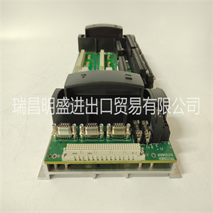


Advanet Advme 7507A VME
内存映射有两种观点:
❏ 本地总线主控器(本地总线)查看的所有资源的映射
内存映射)
❏ VMEbus主机查看的机载资源映射
(VMEbus内存映射)
本地总线内存映射
本地总线内存映射由
传输类型(TT)信号。本地资源响应正常访问
以及中断确认码。
正常地址范围
响应正常地址范围的设备的内存映射为:
如下表所示。正常地址范围由TT定义
本地总线上的信号。对于MVME162,传输类型0、1和2定义了
正常地址范围。表3-1定义了整个地图($00000000至
$FFFFFFFF)。地图的许多区域是用户可编程的,建议
用途见下表。缓存禁止功能可在中编程
MC68xx040 MMU。板载I/O空间必须标记为“缓存禁止”
并在其页表中序列化。表3-2进一步定义了本地
I/O设备。
操作说明
3-4用户手册
3.
注1.重置使解码器能够用于内存映射的该空间,因此
它将解码地址空间$FF800000-$FF9FFFFF和
$00000000-$003FFFFF。必须在中禁用0处的解码
启用DRAM之前的MCchip。DRAM通过以下方式启用:
DRAM控制寄存器,地址$FFF42048,第24位。
PROM/闪存在PROM的低地址空间被禁用
控制寄存器地址为$FFF42040,第20位。
2.该区域可由用户编程。DRAM和SRAM
解码器编程在MCchip中,本地到VMEbus
解码器在VMEchip2和IP中编程
存储器空间在IPIC中编程。
3.尺寸为近似值。
4.缓存禁止取决于映射区域中的设备。
表3-1.本地总线内存映射
访问设备的地址范围端口宽度大小
软件
隐藏物
阻止
笔记
板载可编程DRAM D32 1MB-8MB N 2
可编程SRAM D32 128KB-2MB N 2
可编程VMEbus A32/A24 D32/D16--?4.
可编程IP_a存储器D32-D8 64 KB-8 MB?2, 4
可编程IP_b内存D32-D8 64 KB-8 MB?2, 4
可编程IP_c存储器D32-D8 64 KB-8 MB?2, 4
可编程IP_d存储器D32-D8 64 KB-8 MB?2, 4
$FF800000-$FF9FFFFF闪存/EPROM D32 2 MB N 1,5
$FF1000000-$FFBFFFFF EPROM/闪存D32 2 MB N 6
$FFC00000-$FFCFFFFF未解码D32 1 MB N 7
$FFD00000-$FFDFFFFF未解码D32 1 MB N 7
$FFE00000-$FFE7FFFF SRAM默认D32 512 KB N--
$FFE80000-$FFEFFFF未解码--512 KB N 7
$FFF00000-$FFFEFFFF本地I/O设备
(参见下表)
D32-D8 878 KB Y 3
$FFFF0000-$FFFFFFFF VMEbus A16 D32/D16 64 KB?2, 4
记忆地图
MVME162/D2 3-5
3.
5.EPROM和闪存的大小由MCchip ASIC根据
8位专用总线到32位MPU本地总线。因为
对于某些情况,设备大小小于分配的内存映射
条目,设备内容对这些条目重复。
如果安装了跳线GPIO3,则访问闪存设备。如果
如果未安装GPIO3,则访问EPROM。
6.闪存和EPROM的大小由MCchip ASIC确定
8位专用总线到32位MPU本地总线。因为
对于某些情况,设备大小小于分配的内存映射
条目,设备内容对这些条目重复。
如果安装了跳线GPIO3,则可访问PROM设备。如果
如果未安装GPIO3,则访问闪存。
7.这些区域不解码,除非其中一个可编程
解码器被初始化以解码该空间。如果不是
解码后,对该地址范围的访问将生成本地
总线超时。必须启用本地总线定时器。
表3-2重点介绍了本地总线干线的“本地I/O设备”部分
内存映射。
表3-2本地I/O设备内存映射
访问设备的地址范围、端口宽度和大小注释
$FFF00000-$FFF3FFFF保留--256 KB 4
$FFF40000-$FFF400FF VMEchip2(LCSR)D32 256 B 1,3
$FFF40100-$FFF201FF VMEchip2(GCSR)D32-D8 256 B 1,3
$FFF40200-$FFF40FFF保留--3.5 KB 4,5
$FFF41000-$FFF41FFF保留--4 KB 4
$FFF42000-$FFF42FFF MCchip D32-D8 4 KB 1
$FFF43000-$FFF44FFF保留--8 KB 4
$FFF4500-$FFF45800 SCC#1(Z85230)D8 2 KB 1,2
$FFF45801-$FFF45 FFF SCC#2(Z85230)D8 2 KB 1,2
$FFF46000-$FFF46FFF局域网(82596CA)D32 4 KB 1,6
$FFF47000-$FFF47FFF SCSI(53C710)D32-D8 4 KB 1
$FFF48000-$FFF57FFF保留--64 KB 4
$FFF58000-$FFF5807F IPIC IP_a I/O D16 128 B 1
$FFF5800-$FFF580FF IPIC IP_a ID D16 128 B 1
$FFF58100-$FFF4817F IPIC IP_b I/O D16 128 b 1
$FFF58180-$FFF481FF IPIC IP_b ID读取D16 128 b 1
$FFF58200-$FFF4827F IPIC IP_c I/O D16 128 B 1
操作说明
3-6用户手册
3.
注1.有关寄存器位的完整描述,请参阅数据
特定芯片的表。对于更详细的存储器映射,
请参阅以下详细的外围设备存储器
地图。
2.SCC是位于MCchip专用数据上的8位设备
公共汽车需要字节访问。
$FFF58280-$FFF482FF IPIC IP_c ID D16 128 B 1
$FFF58300-$FFF4837F IPIC IP_d I/O D16 128 B
Advanet Advme 7507A VME
Advanet Advme 7507A VME
here are two points of view for memory maps:
❏ The mapping of all resources as viewed by local bus masters (local bus
memory map)
❏ The mapping of onboard resources as viewed by VMEbus masters
(VMEbus memory map)
Local Bus Memory Map
The local bus memory map is split into different address spaces by the
Transfer Type (TT) signals. The local resources respond to the normal access
and interrupt acknowledge codes.
Normal Address Range
The memory map of devices that respond to the normal address range is
shown in the following tables. The normal address range is defined by the TT
signals on the local bus. For the MVME162, transfer types 0, 1, and 2 define the
normal address range. Table 3-1 defines the entire map ($00000000 to
$FFFFFFFF). Many areas of the map are user-programmable, and suggested
uses are shown in the table. The cache inhibit function is programmable in the
MC68xx040 MMU. The onboard I/O space must be marked ‘‘cache inhibit’’
and serialized in its page table. Table 3-2 further defines the map for the local
I/O devices.
Operating Instructions
3-4 User’s Manual
3
Notes 1. Reset enables the decoder for this space of the memory map so
that it will decode address spaces $FF800000 - $FF9FFFFF and
$00000000 - $003FFFFF. The decode at 0 must be disabled in
the MCchip before DRAM is enabled. DRAM is enabled with
the DRAM Control Register at address $FFF42048, bit 24.
PROM/Flash is disabled at the low address space with PROM
Control Register at address $FFF42040, bit 20.
2. This area is user-programmable. The DRAM and SRAM
decoder is programmed in the MCchip, the local-to-VMEbus
decoders are programmed in the VMEchip2, and the IP
memory space is programmed in the IPIC.
3. Size is approximate.
4. Cache inhibit depends on devices in area mapped.
Table 3-1. Local Bus Memory Map
Address Range Devices Accessed Port Width Size
Software
Cache
Inhibit
Notes
Programmable DRAM on Board D32 1MB-8MB N 2
Programmable SRAM D32 128KB-2MB N 2
Programmable VMEbus A32/A24 D32/D16 -- ? 4
Programmable IP_a Memory D32-D8 64 KB-8 MB ? 2, 4
Programmable IP_b Memory D32-D8 64 KB-8 MB ? 2, 4
Programmable IP_c Memory D32-D8 64 KB-8 MB ? 2, 4
Programmable IP_d Memory D32-D8 64 KB-8 MB ? 2, 4
$FF800000-$FF9FFFFF Flash/EPROM D32 2 MB N 1, 5
$FFA00000-$FFBFFFFF EPROM/Flash D32 2 MB N 6
$FFC00000-$FFCFFFFF Not Decoded D32 1 MB N 7
$FFD00000-$FFDFFFFF Not Decoded D32 1 MB N 7
$FFE00000-$FFE7FFFF SRAM default D32 512 KB N --
$FFE80000-$FFEFFFFF Not Decoded -- 512 KB N 7
$FFF00000-$FFFEFFFF Local I/O Devices
(Refer to next table)
D32-D8 878 KB Y 3
$FFFF0000-$FFFFFFFF VMEbus A16 D32/D16 64 KB ? 2, 4
Memory Maps
MVME162/D2 3-5
3
5. The EPROM and Flash are sized by the MCchip ASIC from an
8-bit private bus to the 32-bit MPU local bus. Because the
device size is less than the allocated memory map for some
entries, the device contents repeat for those entries.
If jumper GPIO3 is installed, the Flash device is accessed. If
GPIO3 is not installed, the EPROM is accessed.
6. The Flash and EPROM are sized by the MCchip ASIC from an
8-bit private bus to the 32-bit MPU local bus. Because the
device size is less than the allocated memory map for some
entries, the device contents repeat for those entries.
If jumper GPIO3 is installed, the PROM device is accessed. If
GPIO3 is not installed, the Flash is accessed.
7. These areas are not decoded unless one of the programmable
decoders are initialized to decode this space. If they are not
decoded, an access to this address range will generate a local
bus timeout. The local bus timer must be enabled.
Table 3-2 focuses on the ‘‘Local I/O Devices’’ portion of the local bus main
memory map.
Table 3-2. Local I/O Devices Memory Map
Address Range Devices Accessed Port Width Size Notes
$FFF00000 - $FFF3FFFF Reserved - - 256 KB 4
$FFF40000 - $FFF400FF VMEchip2 (LCSR) D32 256 B 1, 3
$FFF40100 - $FFF401FF VMEchip2 (GCSR) D32-D8 256 B 1, 3
$FFF40200 - $FFF40FFF Reserved - - 3.5 KB 4, 5
$FFF41000 - $FFF41FFF Reserved - - 4 KB 4
$FFF42000 - $FFF42FFF MCchip D32-D8 4 KB 1
$FFF43000 - $FFF44FFF Reserved - - 8 KB 4
$FFF45000 - $FFF45800 SCC #1 (Z85230) D8 2 KB 1, 2
$FFF45801 - $FFF45FFF SCC #2 (Z85230) D8 2 KB 1, 2
$FFF46000 - $FFF46FFF LAN (82596CA) D32 4 KB 1, 6
$FFF47000 - $FFF47FFF SCSI (53C710) D32-D8 4 KB 1
$FFF48000 - $FFF57FFF Reserved - - 64 KB 4
$FFF58000 - $FFF5807F IPIC IP_a I/O D16 128 B 1
$FFF58080 - $FFF580FF IPIC IP_a ID D16 128 B 1
$FFF58100 - $FFF5817F IPIC IP_b I/O D16 128 B 1
$FFF58180 - $FFF581FF IPIC IP_b ID Read D16 128 B 1
$FFF58200 - $FFF5827F IPIC IP_c I/O D16 128 B 1
Operating Instructions
3-6 User’s Manual
3
Notes 1. For a complete description of the register bits, refer to the data
sheet for the specific chip. For a more detailed memory map,
refer to the following detailed peripheral device memory
maps.
2. The SCC is an 8-bit device located on an MCchip private data
bus. Byte access is required.
$FFF58280 - $FFF582FF IPIC IP_c ID D16 128 B 1
$FFF58300 - $FFF5837F IPIC IP_d I/O D16 128 B 1
$FFF58380 - $FFF583FF IPIC IP_d ID Read D16 128 B 1
$FFF58400 - $FFF584FF IPIC IP_ab I/O D32-D16 256 B 1
$FFF58500 - $FFF585FF IPIC IP_cd I/O D32-D16 256 B 8
$FFF58600 - $FFF586FF IPIC IP_ab I/O Repeated D32-D16 256 B 1
$FFF58700 - $FFF587FF IPIC IP_cd I/O Repeated D32-D16 256 B 8
$FFF58800 - $FFF5887F Reserved - - 128 B 1
$FFF58880 - $FFF588FF Reserved - - 128 B 1
$FFF58900 - $FFF5897F Reserved - - 128 B 1
$FFF58980 - $FFF589FF Reserved - - 128 B 1
$FFF58A00 - $FFF58A7F Reserved - - 128 B 1
$FFF58A80 - $FFF58AFF Reserved - - 128 B 1
$FFF58B00 - $FFF58B7F Reserved - - 128 B 1
$FFF58B80 - $FFF58BFF Reserved - - 128 B 1
$FFF58C00 - $FFF58CFF Reserved - - 256 B 1
$FFF58D00 - $FFF58DFF Reserved - - 256 B 1
$FFF58E00 - $FFF58EFF Reserved - - 256 B 1
$FFF58F00 - $FFF58FFF Reserved - - 256 B 1
$FFFBC000 - $FFFBC01F IPIC Registers D32-D8 2 KB 1
$FFFBC800 - $FFFBC81F Reserved - - 2 KB 1
$FFFBD000 - $FFFBFFFF Reserved - - 12 KB 4
$FFFC0000 - $FFFC7FFF MK48T08 (BBRAM, TOD Clock) D32-D8 32 KB 1
$FFFC8000 - $FFFCBFFF MK48T08 & Disable Flash writes D32-D8 16 KB 1, 7
$FFFCC000 - $FFFCFFFF MK48T08 & Enable Flash writes D32-D8 16 KB 1, 7
$FFFD0000 - $FFFEFFFF Reserved - - 128 KB 4
Table 3-2.
Copyright ©2019-2022 瑞昌明盛自动化设备有限公司 版权所有 赣ICP备2021006016号