


Advme 7507A
字段定义如下:
1.为该结构的修订或版本保留四个字节。这
修订以ASCII格式存储,前两个字节为主要
版本号,后两个字节是次要版本号。
例如,如果此结构的版本为1.0,则此字段包含:
0100
2.在ASCII中为电路板的序列号保留12个字节
总体安排例如,该字段可以包含:
000000470476
3.为ASCII格式的板ID保留16个字节。例如
对于带有MC68040、SCSI、以太网、4MB DRAM和
512KB SRAM,该字段包含:
MVME162-23(10个字符后面是6个空格。)
4.为印刷线路组件(PWA)编号保留16个字节
以ASCII格式分配给该电路板。这包括01-W前缀。这
如果一个集合需要多个板,则用于主逻辑板。
集合中的其他板由该集合的结构定义。对于
例如,对于带有MC68040、SCSI、以太网、4MB的MVME162板
DRAM和512KB SRAM,在修订版A中,PWA字段包含:
01-W3814B01A(12个字符后有四个空格。)
5.四个字节包含以MHz为单位的板速度。前两个字节是
MHz的整数和二个字节是MHz的分数。
例如,对于25.00 MHz板,该字段包含:
2500
6.为以太网地址保留六个字节。地址存储在
十六进制格式。(请参阅4章中的详细说明。)如果
电路板不支持以太网,该字段用零填充。
7.这两个字节是保留的。
8.为本地SCSI ID保留两个字节。SCSI ID存储在
ASCII格式。
9.为印刷线路板(PWB)编号保留8个字节
以ASCII格式分配给内存夹层板。但事实并非如此
包括01-W前缀。例如,对于位于
修订版A,PWB字段包含:
3837B02A
10.为分配给存储器的序列号保留8个字节
ASCII格式的夹层板。
记忆地图
MVME162/D2 3-23
3.
11.为印刷线路板(PWB)编号保留八个字节
以ASCII格式分配给串行端口2个性板。
12.为分配给串行端口2的序列号保留8个字节
ASCII格式的个性板。
13.为电路板标识符保留八个字节,ASCII格式,分配
到可选的一个IndustryPack a。
14.为序列号保留8个字节,ASCII格式,分配
到可选的一个IndustryPack a。
15.为印刷线路板(PWB)编号保留8个字节
分配给可选的一个IndustryPack a。
16.为电路板标识符保留8个字节,ASCII格式,分配
至可选的二个工业包装b。
17.以ASCII格式为序列号保留八个字节,分配
至可选的二个工业包装b。
18.为印刷线路板(PWB)编号保留八个字节
分配给可选的二工业包装b。
19.为电路板标识符保留8个字节,ASCII格式,分配
至可选的三工业包装c。
20.为序列号保留8个字节,ASCII格式,分配
至可选的三工业包装c。
21.为印刷线路板(PWB)编号保留八个字节
分配给可选的三工业包装c。
22.为电路板标识符保留8个字节,ASCII格式,分配
至可选的四工业包装d。
23.以ASCII格式为序列号保留八个字节,分配
至可选的四工业包装d。
24.为印刷线路板(PWB)编号保留八个字节
分配给可选的四个IndustryPack d。
25.保留增长空间(65字节)。这将结构填充到偶数256
字节。
26.区域的后一个字节保留用于校验和(如
MVME162Bug调试包用户手册)用于安全和数据
NVRAM配置区域的完整性。此数据存储在
十六进制格式。
Advme 7507A
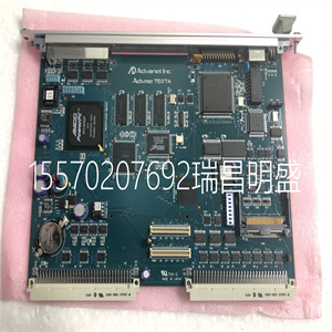
Advme 7507A
The fields are defined as follows:
1. Four bytes are reserved for the revision or version of this structure. This
revision is stored in ASCII format, with the first two bytes being the major
version numbers and the last two bytes being the minor version numbers.
For example, if the version of this structure is 1.0, this field contains:
0100
2. Twelve bytes are reserved for the serial number of the board in ASCII
format. For example, this field could contain:
000000470476
3. Sixteen bytes are reserved for the board ID in ASCII format. For example,
for an MVME162 board with MC68040, SCSI, Ethernet, 4MB DRAM, and
512KB SRAM, this field contains:
MVME162-23 (The 10 characters are followed by six blanks.)
4. Sixteen bytes are reserved for the printed wiring assembly (PWA) number
assigned to this board in ASCII format. This includes the 01-W prefix. This
is for the main logic board if more than one board is required for a set.
Additional boards in a set are defined by a structure for that set. For
example, for an MVME162 board with MC68040, SCSI, Ethernet, 4MB
DRAM, and 512KB SRAM, at revision A, the PWA field contains:
01-W3814B01A (The 12 characters are followed by four blanks.)
5. Four bytes contain the speed of the board in MHz. The first two bytes are
the whole number of MHz and the second two bytes are fractions of MHz.
For example, for a 25.00 MHz board, this field contains:
2500
6. Six bytes are reserved for the Ethernet address. The address is stored in
hexadecimal format. (Refer to the detailed description in Chapter 4.) If the
board does not support Ethernet, this field is filled with zeros.
7. These two bytes are reserved.
8. Two bytes are reserved for the local SCSI ID. The SCSI ID is stored in
ASCII format.
9. Eight bytes are reserved for the printed wiring board (PWB) number
assigned to the memory mezzanine board in ASCII format. This does not
include the 01-W prefix. For example, for a 4MB parity mezzanine at
revision A, the PWB field contains:
3837B02A
10. Eight bytes are reserved for the serial number assigned to the memory
mezzanine board in ASCII format.
Memory Maps
MVME162/D2 3-23
3
11. Eight bytes are reserved for the printed wiring board (PWB) number
assigned to the serial port 2 personality board in ASCII format.
12. Eight bytes are reserved for the serial number assigned to the serial port 2
personality board in ASCII format.
13. Eight bytes are reserved for the board identifier, in ASCII format, assigned
to the optional first IndustryPack a.
14. Eight bytes are reserved for the serial number, in ASCII format, assigned
to the optional first IndustryPack a.
15. Eight bytes are reserved for the printed wiring board (PWB) number
assigned to the optional first IndustryPack a.
16. Eight bytes are reserved for the board identifier, in ASCII format, assigned
to the optional second IndustryPack b.
17. Eight bytes are reserved for the serial number, in ASCII format, assigned
to the optional second IndustryPack b.
18. Eight bytes are reserved for the printed wiring board (PWB) number
assigned to the optional second IndustryPack b.
19. Eight bytes are reserved for the board identifier, in ASCII format, assigned
to the optional third IndustryPack c.
20. Eight bytes are reserved for the serial number, in ASCII format, assigned
to the optional third IndustryPack c.
21. Eight bytes are reserved for the printed wiring board (PWB) number
assigned to the optional third IndustryPack c.
22. Eight bytes are reserved for the board identifier, in ASCII format, assigned
to the optional fourth IndustryPack d.
23. Eight bytes are reserved for the serial number, in ASCII format, assigned
to the optional fourth IndustryPack d.
24. Eight bytes are reserved for the printed wiring board (PWB) number
assigned to the optional fourth IndustryPack d.
25. Growth space (65 bytes) is reserved. This pads the structure to an even 256
bytes.
26. The final one byte of the area is reserved for a checksum (as defined in the
MVME162Bug Debugging Package User’s Manual) for security and data
integrity of the configuration area of the NVRAM. This data is stored in
hexadecimal format.
Copyright ©2019-2022 瑞昌明盛自动化设备有限公司 版权所有 赣ICP备2021006016号