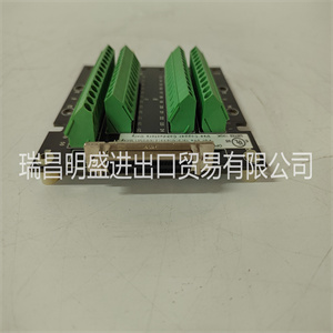


MSK061C-0600-NN-M1-UG1-NNNN
不要收费。
❏ 始终检查正确的极性。
要从模块上拆下电池,请小心地从
插座
安装新电池之前,确保电池引脚清洁。注意
电池极性并将电池压入插座。电池接通时
插座,无需焊接。
机载DRAM
MVME162提供1MB、4MB和8MB DRAM选项。DRAM
架构对于1MB是非交织的,对于4MB和8MB是交织的。
当出现以下情况时,可以通过中断或总线异常启用奇偶校验保护:
检测到奇偶校验错误。DRAM性能在
中的MCchip编程模型中的DRAM存储器控制器
MVME162嵌入式控制器程序员参考指南。
DRAM映射解码器可以编程以适应不同的基础
夹层板的地址和尺寸。板载DRAM被禁用
通过本地总线复位,并且必须在DRAM可以
访问。请参阅MVME162嵌入式系统中的MCchip说明
有关详细编程信息,请参阅控制器程序员参考指南。
大多数DRAM设备在DRAM之前需要一定数量的访问周期
完全可操作。通常情况下,车载刷新可满足此要求
电路和正常DRAM初始化。然而,软件应确保
对每个RAM组执行至少10个初始化周期。
MVME162功能描述
MVME162/D2 4-5
4.
电池备份RAM和时钟
MVME162上使用了MK48T08 RAM和时钟芯片
提供时钟、振荡器、晶体、电源故障检测、存储器
写保护、8KB RAM和一个28针封装中的电池。时钟
以BCD 24小时提供秒、分钟、小时、天、日期、月和年
总体安排28天、29天(闰年)和30天月的修正为
自动生成。时钟不会产生中断。虽然
MK48T08是一个8位设备,由MCchip提供的接口支持
对MK48T08的8位、16位和32位访问。请参阅MCchip说明
在第3章和MK48T08数据表中,详细编程和
电池寿命信息。
VMEbus接口和VMEchip2
可选的VMEchip2提供本地总线到VMEbus和VMEbus到本地总线接口。VMEchip2还可以提供VMEbus系统
控制器功能。参考MVME162嵌入式控制器编程器
详细编程信息的参考指南。参考MVME162
嵌入式控制器的引脚分配支持信息手册
VMEbus背板连接器P1和P2。
注意,不使用VMEchip2中的中止开关逻辑。GPI输入
不使用位于$FFF40088位7-0的VMEchip2。这个
中止开关中断集成在MCchip ASIC的位置
$FFF42043。GPI输入在位置集成到MCchip ASIC
$FFF420C,第23-16位。
I/O接口
MVME162为许多系统应用提供板载I/O。输入/输出
功能包括串行端口、工业包(IP)接口和可选
LAN以太网收发器和SCSI大容量存储设备的接口。
串行通信接口
MVME162使用Zilog Z85230串行端口控制器实现这两种功能
串行通信接口。每个接口支持CTS、DCD、RTS,
以及DTR控制信号以及TxD和RxD发送/接收数据
以及TxC/RxC同步时钟信号。Z85230支持:
同步(SDLC/HDLC)和异步协议。MVME162
硬件支持110B/s到38.4K的异步串行波特率
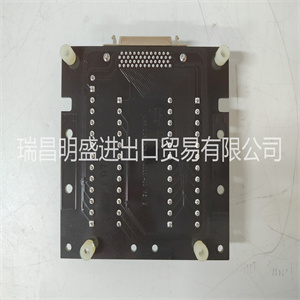
MSK061C-0600-NN-M1-UG1-NNNN
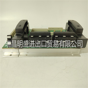
MSK061C-0600-NN-M1-UG1-NNNN
Do not charge.
❏ Always check proper polarity.
To remove the battery from the module, carefully pull the battery from the
socket.
Before installing a new battery, ensure that the battery pins are clean. Note the
battery polarity and press the battery into the socket. When the battery is in
the socket, no soldering is required.
Onboard DRAM
The MVME162 offers a 1MB, a 4MB, and an 8MB DRAM option. The DRAM
architecture is non-interleaved for 1MB and interleaved for 4MB and 8MB.
Parity protection can be enabled with interrupts or bus exception when a
parity error is detected. DRAM performance is specified in the section on the
DRAM Memory Controller in the MCchip Programming Model in the
MVME162 Embedded Controller Programmer’s Reference Guide.
The DRAM map decoder can be programmed to accommodate different base
address(es) and sizes of mezzanine boards. The onboard DRAM is disabled
by a local bus reset and must be programmed before the DRAM can be
accessed. Refer to the MCchip description in the MVME162 Embedded
Controller Programmer’s Reference Guide for detailed programming information.
Most DRAM devices require some number of access cycles before the DRAMs
are fully operational. Normally this requirement is met by the onboard refresh
circuitry and normal DRAM initialization. However, software should insure
that a minimum of 10 initialization cycles are performed to each bank of RAM.
MVME162 Functional Description
MVME162/D2 4-5
4
Battery Backed Up RAM and Clock
An MK48T08 RAM and clock chip is used on the MVME162. This chip
provides a time-of-day clock, oscillator, crystal, power fail detection, memory
write protection, 8KB of RAM, and a battery in one 28-pin package. The clock
provides seconds, minutes, hours, day, date, month, and year in BCD 24-hour
format. Corrections for 28-, 29- (leap year), and 30-day months are
automatically made. No interrupts are generated by the clock. Although the
MK48T08 is an 8- bit device, the interface furnished by the MCchip supports
8-, 16-, and 32-bit accesses to the MK48T08. Refer to the MCchip description
in Chapter 3 and to the MK48T08 data sheet for detailed programming and
battery life information.
VMEbus Interface and VMEchip2
The optional VMEchip2 provides the local-bus-to-VMEbus and VMEbus-tolocal-bus interfaces. The VMEchip2 can also provide the VMEbus system
controller functions. Refer to the MVME162 Embedded Controller Programmer’s
Reference Guide for detailed programming information. Refer to the MVME162
Embedded Controller Support Information manual for the pin assignments of
VMEbus backplane connectors P1 and P2.
Note that the ABORT switch logic in the VMEchip2 is not used. The GPI inputs
to the VMEchip2 which are located at $FFF40088 bits 7-0 are not used. The
ABORT switch interrupt is integrated into the MCchip ASIC at location
$FFF42043. The GPI inputs are integrated into the MCchip ASIC at location
$FFF4202C, bits 23-16.
I/O Interfaces
The MVME162 provides onboard I/O for many system applications. The I/O
functions include serial ports, IndustryPack (IP) interfaces, and optional
interfaces for LAN Ethernet transceivers and SCSI mass storage devices.
Serial Communications Interface
The MVME162 uses a Zilog Z85230 serial port controller to implement the two
serial communications interfaces. Each interface supports CTS, DCD, RTS,
and DTR control signals as well as the TxD and RxD transmit/receive data
signals, and TxC/RxC synchronous clock signals. The Z85230 supports
synchronous (SDLC/HDLC) and asynchronous protocols. The MVME162
hardware supports asynchronous serial baud rates of 110B/s to 38.4K
Copyright ©2019-2022 瑞昌明盛自动化设备有限公司 版权所有 赣ICP备2021006016号