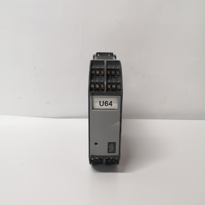


GJR2367400R0100 89NU03A-E 89NU03E 控制器驱动板
1特点
1•高增益带宽产品:5.5 GHz
•失补偿,增益≥ 7 V/V(稳定)
•超低偏置电流MOSFET输入:10 pA
•低输入电压噪声:2.5 nV/√赫兹
•转换速率:2000 V/µs
•低输入电容:
–共模:0.6 pF
–差分:0.2 pF
•宽输入共模范围:
–正极电源1.4 V
–包括负电源
•TIA配置中的2.5 VPP输出摆动
•电源电压范围:3.3 V至5.25 V
•静态电流:20.5 mA
•提供8引脚WSON封装
•温度范围:-40至+125°C
2.申请
•高速跨阻放大器
•激光测距
•激光雷达接收器
•液位变送器(光学)
•光学时域反射计(OTDR)
•分布式温度传感
•3D扫描仪
•飞行时间(ToF)系统
•自动驾驶系统
间隔物
3.说明
OPA858是一种宽带、低噪声、可操作的
宽带CMOS输入放大器
跨阻抗和电压放大器应用。
当设备配置为跨阻抗时
放大器(TIA),5.5GHz增益带宽产品
(GBWP)支持要求高闭合环路带宽的应用,跨阻抗增益为数十
至数百kΩs范围。
下图显示了带宽和
OPA858的噪声性能与
放大器处于以下状态时的光电二极管电容:
配置为TIA。总噪声计算如下:
带宽范围从DC扩展到
计算左侧刻度上的f-3dB频率。这个
OPA858封装具有反馈引脚(FB),该引脚:
简化之间的反馈网络连接
输入和输出。
OPA858被优化用于光学离光时间(ToF)系统,如图所示
下面是OPA858与TDC7201一起使用的位置
时间到数字转换器。OPA858可用于:
高速高分辨率激光雷达系统
模数转换器(ADC)和差分
输出放大器,如THS4541或LMH5401
驱动ADC。
设备信息(1)
零件号包装体尺寸(NOM)
OPA858 WSON(8)2.00 mm×2.00毫米
(1) 有关所有可用的软件包,请参阅
数据表的结尾。
高速飞行时间接收机
光电二极管帽
GJR2367400R0100 89NU03A-E 89NU03E 控制器驱动板
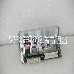
GJR2367400R0100 89NU03A-E 89NU03E 控制器驱动板
1 Features
1• High Gain Bandwidth Product: 5.5 GHz
• Decompensated, Gain ≥ 7 V/V (Stable)
• Ultra-Low Bias Current MOSFET Inputs: 10 pA
• Low Input Voltage Noise: 2.5 nV/√Hz
• Slew rate: 2000 V/µs
• Low Input Capacitance:
– Common-Mode: 0.6 pF
– Differential: 0.2 pF
• Wide Input Common-Mode Range:
– 1.4 V from Positive Supply
– Includes Negative Supply
• 2.5 VPP Output Swing in TIA Configuration
• Supply Voltage Range: 3.3 V to 5.25 V
• Quiescent Current: 20.5 mA
• Available in 8-Pin WSON Package
• Temperature Range: –40 to +125°C
2 Applications
• High-Speed Transimpedance Amplifier
• Laser Distance Measurement
• Lidar Receivers
• Level Transmitter (Optical)
• Optical Time Domain Reflectometry (OTDR)
• Distributed Temperature Sensing
• 3D Scanner
• Time-of-Flight (ToF) Systems
• Autonomous Driving Systems
spacer
3 Description
The OPA858 is a wideband, low-noise, operational
amplifier with CMOS inputs for wideband
transimpedance and voltage amplifier applications.
When the device is configured as a transimpedance
amplifier (TIA), the 5.5-GHz gain bandwidth product
(GBWP) enables applications requiring high closedloop bandwidths at transimpedance gains in the tens
to hundreds of kΩs range.
The graph below demonstrates the bandwidth and
noise performance of the OPA858 as a function of
the photodiode capacitance when the amplifier is
configured as a TIA. The total noise is calculated over
a bandwidth range extending from DC to the
calculated f-3dB frequency on the left-hand scale. The
OPA858 package features a feedback pin (FB) that
simplifies the feedback network connection between
the input and the output.
The OPA858 is optimized for use in optical Time-ofFlight (ToF) systems like the one shown in the figure
below where the OPA858 is used with the TDC7201
time-to-digital converter. The OPA858 can be used in
high-resolution LIDAR systems with a high-speed
analog-to-digital converter (ADC) and a differential
output amplifier like the THS4541 or LMH5401 to
drive the ADC.
Device Information(1)
PART NUMBER PACKAGE BODY SIZE (NOM)
OPA858 WSON (8) 2.00 mm × 2.00 mm
(1) For all available packages, see the orderable addendum at
the end of the data sheet.
High-Speed Time-of-Flight Receiver
Photodiode Cap
Copyright ©2019-2022 瑞昌明盛自动化设备有限公司 版权所有 赣ICP备2021006016号