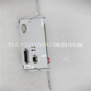


Bailey Infi 90 多功能处理器模块 IMMFP02 IMMFP 02
设备输入类型小稳定
获得
电压噪声
(nV/√赫兹)
投入
电容(pF)
增益带宽
(GHz)
OPA858 CMOS 7 V/V 2.5 0.8 5.5
OPA855双极7 V/V 0.98 0.8 8
LMH6629双极10 V/V 0.69 5.7 4
6引脚配置和功能
DSG包
带外露热垫的8引脚WSON
顶视图
NC-无内部连接
引脚功能
别针
I/O描述
姓名。
FB 1 I至放大器输出的反馈连接
IN–3 I反相输入
IN+4 I非反相输入
NC 2-不连接
输出6 O放大器输出
PD 8 I
关闭连接。PD=逻辑低=断电模式;PD=逻辑高=正常
活动
VS–5-负电压电源
VS+7-正电压电源
热垫-将热垫连接到VS–
4.
OPA858
SBOS629A–2018年4月–2018年7月修订www.ti.com
产品文件夹链接:OPA858
提交文件反馈版权©2018,德克萨斯仪器公司
(1) 超过大额定值的应力可能会对设备造成久性损坏。这些是压力评级
仅限于,不意味着设备在这些或任何其他条件下的功能运行超出推荐条件
操作条件。长时间暴露在大额定条件下可能会影响设备可靠性。
(2) 电迁移极限的长期连续输出电流。
7.规格
7.1大额定值
超工作自由空气温度范围(除非另有说明)(1)
小大单位
VS总电源电压(VS+–VS-)5.5
五、
VIN+,VIN–输入电压(VS-)–0.5(VS++0.5
VID差分输入电压1
VOUT输出电压(VS-)–0.5(VS+)+0.5
IIN连续输入电流±10
妈妈
IOUT连续输出电流(2)±100
TJ结温度150
TA工作自由空气温度125°C
TSTG储存温度–65 150
(1) JEDEC文件JEP155指出,500-V HBM允许使用标准ESD控制工艺进行安全制造。
(2) JEDEC文件JEP157指出,250-V CDM允许使用标准ESD控制工艺进行安全制造。
7.2 ESD额定值
价值单位
V(ESD)静电放电
人体模型(HBM),符合ANSI/ESDA/JEDEC JS-001(1)±1000
充电装置型号(CDM),符合JEDEC规范JESD22-V
C101(2)±1500
7.3推荐操作条件
超工作自由空气温度范围(除非另有说明)
小标称大单位
VS总电源电压(VS+–VS-)3.3 5 5.25 V
(1) 有关传统和新热计量的更多信息,请参阅半导体和IC封装热计量应用程序
汇报
7.4热信息
热计量(1)
OPA858
DSG(WSON)单元
8针
RθJA结至环境热阻80.1°C/W
RθJC(顶部)结至外壳(顶部)热阻100°C/W
RθJB接线板热阻45°C/W
ψJT结至顶部表征参数6.8°C/W
ψJB结至板特性参数45.2°C/W
RθJC(bot)结至外壳(底部)热阻22.7°C/W
5.
OPA858
www.ti.com.SBOS629A–2018年4月–2018年7月修订
产品文件夹链接:OPA858
版权所有©2018,德克萨斯仪器公司提交文件反馈
(1) 测试水平(通过表征和模拟设置的所有值):(A)在25°C下进行100%测试,通过表征和
模拟(B) 未在生产中测试,通过特征和模拟设定的限值;(C) 典型值仅供参考。
7.5电气特性
VS+=5 V,VS–=0 V,G=7 V/V,RF=453Ω,输入共模偏置在中间电源,RL=200Ω,参考输出负载
供应中期,TA=25℃(除非另有说明)
参数测试条件小典型大单元测试
级别(1)
交流性能
SSBW小信号带宽VOUT=100 mVPP 1.2 GHz C
LSBW大信号带宽VOUT=2 VPP 600 MHz C
GBWP增益带宽积5.5GHz C
0.1-dB平坦度的带宽130 MHz C
SR转换率(10%-90%)VOUT=2-V阶跃2000 V/µs C
tr上升时间VOUT=100 mV阶跃0.3 ns C
tf下降时间VOUT=100 mV阶跃0.3 ns C
0.1%VOUT=2-V阶跃8 ns C的稳定时间
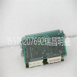
Bailey Infi 90 多功能处理器模块 IMMFP02 IMMFP 02
Bailey Infi 90 多功能处理器模块 IMMFP02 IMMFP 02
DEVICE INPUT TYPE MINIMUM STABLE
GAIN
VOLTAGE NOISE
(nV/√Hz)
INPUT
CAPACITANCE (pF)
GAIN BANDWIDTH
(GHz)
OPA858 CMOS 7 V/V 2.5 0.8 5.5
OPA855 Bipolar 7 V/V 0.98 0.8 8
LMH6629 Bipolar 10 V/V 0.69 5.7 4
6 Pin Configuration and Functions
DSG Package
8-Pin WSON With Exposed Thermal Pad
Top View
NC - no internal connection
Pin Functions
PIN
I/O DESCRIPTION
NAME NO.
FB 1 I Feedback connection to output of amplifier
IN– 3 I Inverting input
IN+ 4 I Noninverting input
NC 2 — Do not connect
OUT 6 O Amplifier output
PD 8 I
Power down connection. PD = logic low = power off mode; PD = logic high = normal
operation
VS– 5 — Negative voltage supply
VS+ 7 — Positive voltage supply
Thermal pad — Connect the thermal pad to VS–
4
OPA858
SBOS629A –APRIL 2018–REVISED JULY 2018 www.ti.com
Product Folder Links: OPA858
Submit Documentation Feedback Copyright © 2018, Texas Instruments Incorporated
(1) Stresses beyond those listed under Absolute Maximum Ratings may cause permanent damage to the device. These are stress ratings
only, which do not imply functional operation of the device at these or any other conditions beyond those indicated under Recommended
Operating Conditions. Exposure to absolute-maximum-rated conditions for extended periods may affect device reliability.
(2) Long-term continuous output current for electromigration limits.
7 Specifications
7.1 Absolute Maximum Ratings
over operating free-air temperature range (unless otherwise noted)(1)
MIN MAX UNIT
VS Total supply voltage (VS+ – VS–) 5.5
V
VIN+, VIN– Input voltage (VS–) – 0.5 (VS+) + 0.5
VID Differential input voltage 1
VOUT Output voltage (VS–) – 0.5 (VS+) + 0.5
IIN Continuous input current ±10
mA
IOUT Continuous output current(2) ±100
TJ Junction temperature 150
TA Operating free-air temperature 125 °C
TSTG Storage temperature –65 150
(1) JEDEC document JEP155 states that 500-V HBM allows safe manufacturing with a standard ESD control process.
(2) JEDEC document JEP157 states that 250-V CDM allows safe manufacturing with a standard ESD control process.
7.2 ESD Ratings
VALUE UNIT
V(ESD) Electrostatic discharge
Human-body model (HBM), per ANSI/ESDA/JEDEC JS-001(1) ±1000
Charged-device model (CDM), per JEDEC specification JESD22- V
C101(2) ±1500
7.3 Recommended Operating Conditions
over operating free-air temperature range (unless otherwise noted)
MIN NOM MAX UNIT
VS Total supply voltage (VS+ – VS–) 3.3 5 5.25 V
(1) For more information about traditional and new thermal metrics, see the Semiconductor and IC Package Thermal Metrics application
report.
7.4 Thermal Information
THERMAL METRIC(1)
OPA858
DSG (WSON) UNIT
8 PINS
RθJA Junction-to-ambient thermal resistance 80.1 °C/W
RθJC(top) Junction-to-case (top) thermal resistance 100 °C/W
RθJB Junction-to-board thermal resistance 45 °C/W
ψJT Junction-to-top characterization parameter 6.8 °C/W
ψJB Junction-to-board characterization parameter 45.2 °C/W
RθJC(bot) Junction-to-case (bottom) thermal resistance 22.7 °C/W
5
OPA858
www.ti.com SBOS629A –APRIL 2018–REVISED JULY 2018
Product Folder Links: OPA858
Copyright © 2018, Texas Instruments Incorporated Submit Documentation Feedback
(1) Test levels (all values set by characterization and simulation): (A) 100% tested at 25°C, overtemperature limits by characterization and
simulation; (B) Not tested in production, limits set by characterization and simulation; (C) Typical value only for information.
7.5 Electrical Characteristics
VS+ = 5 V, VS– = 0 V, G = 7 V/V, RF = 453 Ω, input common-mode biased at midsupply, RL = 200 Ω, output load is referenced
to midsupply, and TA = 25℃ (unless otherwise noted)
PARAMETER TEST CONDITIONS MIN TYP MAX UNIT TEST
LEVEL(1)a
AC PERFORMANCE
SSBW Small-signal bandwidth VOUT = 100 mVPP 1.2 GHz C
LSBW Large-signal bandwidth VOUT = 2 VPP 600 MHz C
GBWP Gain-bandwidth product 5.5 GHz C
Bandwidth for 0.1-dB flatness 130 MHz C
SR Slew rate (10% - 90%) VOUT = 2-V step 2000 V/µs C
tr Rise time VOUT = 100-mV step 0.3 ns C
tf Fall time VOUT = 100-mV step 0.3 ns C
Settling time to 0.1% VOUT = 2-V step 8 ns C
Copyright ©2019-2022 瑞昌明盛自动化设备有限公司 版权所有 赣ICP备2021006016号