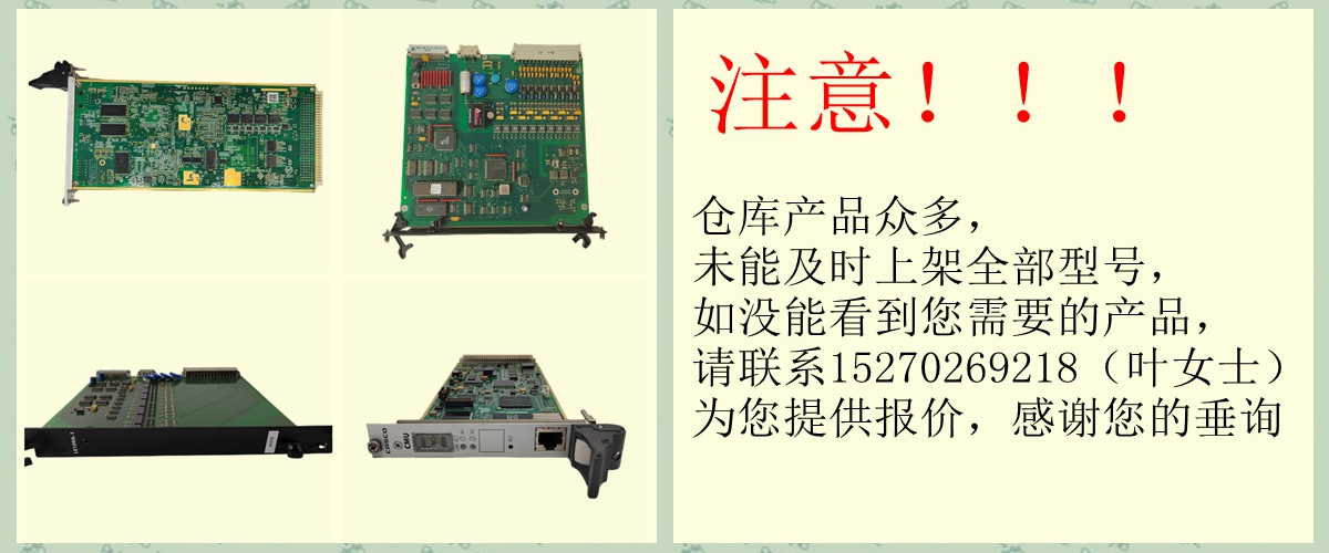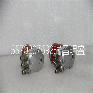


NXPP-06C NXPP06C 应用于DCS系统适配器主板
详细说明
9.1概述
OPA858的超宽、5.5GHz增益带宽积(GBWP),结合宽带电压
2.5 nV的噪声/√Hz,为宽带跨阻抗应用、高速数据提供了可行的放大器
以及具有需要低噪声和高增益前端的弱信号输入的应用。
OPA858结合了多种功能以优化动态性能。除了宽、小信号
带宽,OPA858具有600 MHz的大信号带宽(VOUT=2 VPP)和2000 V/µs的转换速率。
OPA858采用2毫米×2毫米的8引脚WSON封装,具有反馈(FB)引脚
放大器输出和反相输入之间的反馈网络连接。an上的过电容
放大器输入引脚可以减少相位裕度,从而导致不稳定性。这一问题在以下情况下加剧:
宽带放大器,如OPA858。为了减少输入节点上杂散电容的影响,OPA859
引脚输出具有反馈和反相输入引脚之间的隔离引脚(NC),这增加了物理性能
从而减少高频下的寄生耦合。OPA858还具有非常
低电容输入级,仅占总输入电容的0.8-pF。
9.2功能框图
OPA858是一款经典的电压反馈运算放大器(运算放大器),具有两个高阻抗输入和
低阻抗输出。支持标准应用电路,如图46所示的两个基本选项
以及图47。每种配置的直流工作点通过参考电压(VREF)进行电平偏移,
其在单电源操作中通常被设置为中等供应。VREF通常在分体式电源中接地
应用。
图46.同相放大器
图47.反相放大器
2018年4月-2018年7月修订www.ti.com
产品文件夹链接:OPA858
提交文件反馈版权©2018,德克萨斯仪器公司
9.3特征描述
9.3.1输入和ESD保护
OPA858采用低压、高速、BiCMOS工艺制造。内部结击穿
这些小型几何器件的电压较低,因此,所有器件引脚都受到内部保护
电源的ESD保护二极管如图48所示。之间有两个反并联二极管
放大器的输入,在过量程或故障条件下箝位输入。
图48内部ESD结构
9.3.2反馈引脚
OPA858引脚布局经过优化,以小化寄生电感和电容,这在高速模拟设计中至关重要。FB引脚(引脚1)内部连接到放大器的输出。FB引脚为
通过非连接(NC)引脚(引脚2)与放大器的反相输入(引脚3)分离。NC引脚必须为
左浮动。这种引脚布局有两个优点:
1.反馈电阻器(RF)可连接在封装同一侧的FB和IN–引脚之间(参见
图49)。
2.NC引脚产生的隔离通过以下方式小化FB和IN引脚之间的电容耦合:
增加pi之间的物理间隔
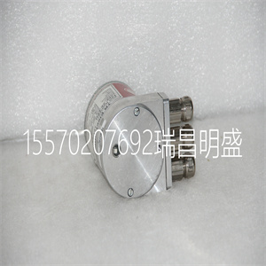
NXPP-06C NXPP06C 应用于DCS系统适配器主板
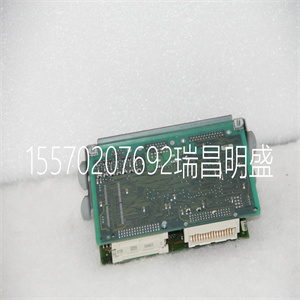
NXPP-06C NXPP06C 应用于DCS系统适配器主板
Detailed Description
9.1 Overview
The ultra-wide, 5.5-GHz gain bandwidth product (GBWP) of the OPA858, combined with the broadband voltage
noise of 2.5 nV/√Hz, produces a viable amplifier for wideband transimpedance applications, high-speed data
acquisition systems, and applications with weak signal inputs that require low-noise and high-gain front ends.
The OPA858 combines multiple features to optimize dynamic performance. In addition to the wide, small-signal
bandwidth, the OPA858 has 600 MHz of large signal bandwidth (VOUT = 2 VPP) and a slew rate of 2000 V/µs.
The OPA858 is offered in a 2-mm × 2-mm, 8-pin WSON package that features a feedback (FB) pin for a simple
feedback network connection between the amplifiers output and inverting input. Excess capacitance on an
amplifiers input pin can reduce phase margin causing instability. This problem is exacerbated in the case of very
wideband amplifiers like the OPA858. To reduce the effects of stray capacitance on the input node, the OPA858
pinout features an isolation pin (NC) between the feedback and inverting input pins that increases the physical
spacing between them thereby reducing parasitic coupling at high frequencies. The OPA858 also features a very
low capacitance input stage with only 0.8-pF of total input capacitance.
9.2 Functional Block Diagram
The OPA858 is a classic, voltage feedback operational amplifier (op amp) with two high-impedance inputs and a
low-impedance output. Standard application circuits are supported, like the two basic options shown in Figure 46
and Figure 47. The DC operating point for each configuration is level-shifted by the reference voltage (VREF),
which is typically set to midsupply in single-supply operation. VREF is typically connected to ground in split-supply
applications.
Figure 46. Noninverting Amplifier
Figure 47. Inverting Amplifier
APRIL 2018–REVISED JULY 2018 www.ti.com
Product Folder Links: OPA858
Submit Documentation Feedback Copyright © 2018, Texas Instruments Incorporated
9.3 Feature Description
9.3.1 Input and ESD Protection
The OPA858 is fabricated on a low-voltage, high-speed, BiCMOS process. The internal, junction breakdown
voltages are low for these small geometry devices, and as a result, all device pins are protected with internal
ESD protection diodes to the power supplies as Figure 48 shows. There are two antiparallel diodes between the
inputs of the amplifier that clamp the inputs during an overrange or fault condition.
Figure 48. Internal ESD Structure
9.3.2 Feedback Pin
The OPA858 pin layout is optimized to minimize parasitic inductance and capacitance, which is critical in highspeed analog design. The FB pin (pin 1) is internally connected to the output of the amplifier. The FB pin is
separated from the inverting input of the amplifier (pin 3) by a no connect (NC) pin (pin 2). The NC pin must be
left floating. There are two advantages to this pin layout:
1. A feedback resistor (RF) can connect between the FB and IN– pin on the same side of the package (see
Figure 49) rather than going around the package.
2. The isolation created by the NC pin minimizes the capacitive coupling between the FB and IN– pins by
increasing the physical separation between the pi
Copyright ©2019-2022 瑞昌明盛自动化设备有限公司 版权所有 赣ICP备2021006016号