

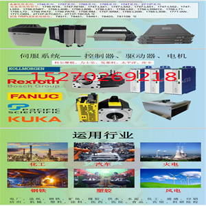


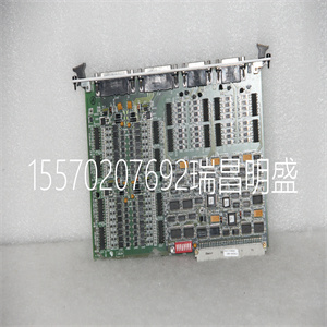
61580-002S 1-061579-001 数字量扩展PC卡用于控制电力
功能描述(续)
9.3.3宽增益带宽积
图10显示了OPA858的开环幅度和相位响应。计算增益带宽
通过确定AOL为60 dB的频率并将该频率乘以
系数1000。AOL响应中的二个极点出现在幅值超过0 dB之前,并且
合成相位裕度小于0°。这表示增益为0dB(1V/V)时的不稳定性。放大器不是
单位增益稳定被称为失补偿放大器。与单位增益稳定放大器相比,失补偿放大器通常具有更高的增益带宽积、更高的转换速率和更低的电压噪声
静态功耗相同。
图50显示了作为温度函数的OPA858的开环幅度(AOL)。结果表明:
温度变化小。OPA858的相位裕度配置为7 V/V的噪声增益(16.9
dB)在温度范围内接近55°。类似地,图51显示了OPA858的AOL幅度为
工艺变化的函数。结果显示了标称工艺角和变化的AOL曲线
标称值的一个标准偏差。模拟结果表明,相位裕度差小于1°
当放大器配置为7V/V的增益时,在工艺变化的标准偏差内。
OPA858的主要应用之一是用作高速跨阻抗放大器(TIA),如图59所示
显示。TIA的低频噪声增益为0dB(1V/V)。在高频下,总输入的比率
电容和反馈电容设置噪声增益。为了大化TIA闭环带宽
反馈电容通常小于输入电容,这意味着高频噪声
增益大于0 dB。因此,配置为TIA的运算放大器不需要单位增益稳定,这
使失补偿放大器成为TIA的可行选择。关于跨阻抗,你需要知道什么
放大器–1部分和您需要了解的跨阻抗放大器–2部分描述
更详细地描述跨阻抗放大器补偿。
图50开环增益与温度图51开环增益和工艺变化
9.3.4转换速率和输出级
除了宽带宽外,OPA858还具有2000 V/µs的高转换速率。转换速率是一个关键
具有窄亚10 ns脉冲的高速脉冲应用中的参数,如光时域
反射计(OTDR)和激光雷达。OPA858的高转换速率意味着该设备准确
再现如图20所示的2-V、亚ns脉冲边缘。OPA858的宽带宽和转换速率
使其成为高速信号链前端的理想放大器。
图52显示了OPA858的开环输出阻抗
61580-002S 1-061579-001 数字量扩展PC卡用于控制电力
61580-002S 1-061579-001 数字量扩展PC卡用于控制电力
Feature Description (continued)
9.3.3 Wide Gain-Bandwidth Product
Figure 10 shows the open-loop magnitude and phase response of the OPA858. Calculate the gain bandwidth
product of any op amp by determining the frequency at which the AOL is 60 dB and multiplying that frequency by
a factor of 1000. The second pole in the AOL response occurs before the magnitude crosses 0 dB, and the
resultant phase margin is less than 0°. This indicates instability at a gain of 0 dB (1 V/V). Amplifiers that are not
unity-gain stable are known as decompensated amplifiers. Decompensated amplifiers typically have higher gainbandwidth product, higher slew rate, and lower voltage noise, compared to a unity-gain stable amplifier with the
same amount of quiescent power consumption.
Figure 50 shows the open-loop magnitude (AOL) of the OPA858 as a function of temperature. The results show
minimal variation over temperature. The phase margin of the OPA858 configured in a noise gain of 7 V/V (16.9
dB) is close to 55° across temperature. Similarly Figure 51 shows the AOL magnitude of the OPA858 as a
function of process variation. The results show the AOL curve for the nominal process corner and the variation
one standard deviation from the nominal. The simulated results suggest less than 1° of phase margin difference
within a standard deviation of process variation when the amplifier is configured in a gain of 7 V/V.
One of the primary applications for the OPA858 is as a high-speed transimpedance amplifier (TIA), as Figure 59
shows. The low-frequency noise gain of a TIA is 0 dB (1 V/V). At high frequencies the ratio of the total input
capacitance and the feedback capacitance set the noise gain. To maximize the TIA closed-loop bandwidth, the
feedback capacitance is typically smaller than the input capacitance, which implies that the high-frequency noise
gain is greater than 0 dB. As a result, op amps configured as TIAs are not required to be unity-gain stable, which
makes a decompensated amplifier a viable option for a TIA. What You Need To Know About Transimpedance
Amplifiers – Part 1 and What You Need To Know About Transimpedance Amplifiers – Part 2 describe
transimpedance amplifier compensation in greater detail.
Figure 50. Open-Loop Gain vs Temperature Figure 51. Open-Loop Gain vs Process Variation
9.3.4 Slew Rate and Output Stage
In addition to wide bandwidth, the OPA858 features a high slew rate of 2000 V/µs . The slew rate is a critical
parameter in high-speed pulse applications with narrow sub 10-ns pulses such as Optical Time-Domain
Reflectometry (OTDR) and LIDAR. The high slew rate of the OPA858 implies that the device accurately
reproduces a 2-V, sub-ns pulse edge as seen in Figure 20. The wide bandwidth and slew rate of the OPA858
make it an ideal amplifier for high-speed, signal-chain front ends.
Figure 52 shows the open-loop output impedance of the OPA858 as
Copyright ©2019-2022 瑞昌明盛自动化设备有限公司 版权所有 赣ICP备2021006016号