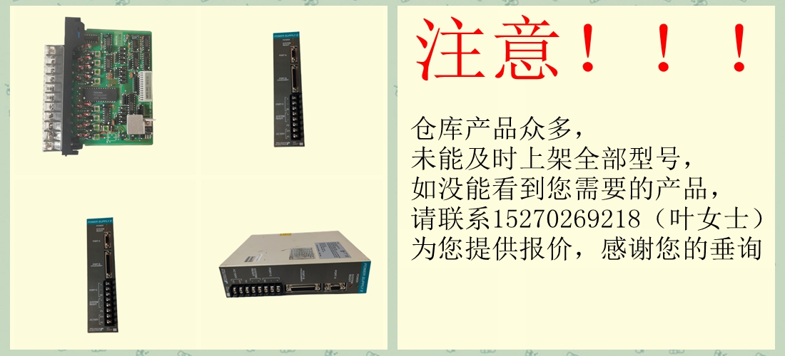


AI05 模拟输入模块 8 通道隔离
OPA858可配置单面电源或分体式电源,如图63所示。分体式电源
使用输入共模设置为接地的平衡电源的操作简化了实验室测试,因为大多数
信号发生器、网络分析仪、频谱分析仪和其他实验室设备通常参考输入和
输出接地。在信号绕地摆动的系统中,分路供电操作是优选的。
然而,该系统需要两个供电轨。在分路供电操作中,热垫必须连接到
负电源。
较新的系统使用单个电源来提高效率并降低额外电源的成本。
OPA858可与单个正电源(接地负电源)一起使用,无需改变
如果输入共模和输出摆幅在设备的线性操作中偏置,则性能。到
将电路从分体式电源更改为单电源配置,将所有电压电平移动一半
电源导轨之间的差异。在这种情况下,热垫必须接地。
9.4.2断电模式
OPA858具有断电模式,以减少静态电流以节省功率。图23和
图24显示了当PD引脚在禁用和启用之间切换时,OPA858的瞬态响应
美国。
PD禁用和启用阈值电压参考负电源。如果放大器是
配置3.3 V的正电源和接地的负电源,然后禁用和启用
阈值电压分别为0.65V和1.8V。如果放大器配置有±1.65 V电源,则
禁用和启用阈值电压分别为-1 V和0.15 V。如果放大器配置为:
±2.5-V电源,则阈值电压为-1.85 V和-0.7 V。
图54显示了当PD引脚从启用状态向下扫描时,典型放大器的开关行为
变为禁用状态。类似地,图55显示了典型放大器的开关行为,如PD引脚所示
从禁用状态向上扫描到启用状态。之间切换阈值的微小差异
下扫和上扫是由于放大器中设计的滞后,以增加其抗干扰性
PD引脚上的噪声。
图54.开关阈值(PD引脚从高电平扫描
低)
图55.开关阈值(PD引脚从低扫描
高)
将PD引脚连接到低电平将禁用放大器,并将输出置于高阻抗状态。当
放大器配置为非反相放大器,反馈(RF)和增益(RG)电阻网络形成
放大器输出的并联负载。为了保护放大器的输入级,
反相和非反相输入引脚之间的背对背保护二极管,如图48所示。当
放大器输入引脚之间的差分电压超过二极管电压降,则在输入之间产生额外的低阻抗路径
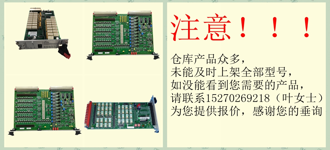
AI05 模拟输入模块 8 通道隔离
AI05 模拟输入模块 8 通道隔离
Xopa858 can be configured with single-sided power supply or split power supply, as shown in Figure 63. Split power supply
Operation using a balanced power supply with input common mode set to ground simplifies laboratory testing because most
Signal generators, network analyzers, spectrum analyzers and other laboratory equipment (usually reference inputs); and
The output is grounded. In a system in which the signal swings around the ground, a shunt power supply operation is preferable.
However, the system requires two power rails. In shunt operation, the thermal pad must be connected to
Negative power supply.
Newer systems use a single power source to improve efficiency and reduce the cost of additional power.
Opa858 can be used with a single positive power supply (grounded negative power supply) without change
If the input common mode and the output swing are biased in the linear operation of the device, the performance is improved. reach
Change the circuit from a split power supply to a single power supply configuration, shifting all voltage levels by half
Difference between power rails. In this case, the thermal pad must be grounded.
9.4.2 power off mode
Opa858 has a power-off mode to reduce quiescent current to save power. Figure 23 and
Figure 24 shows the transient response of opa858 when the PD pin switches between disabled and enabled
U.S.A.
PD disables and enables the threshold voltage reference negative power supply. If the amplifier is
Configure 3.3 V positive power supply and grounded negative power supply, then disable and enable
The threshold voltages are 0.65v and 1.8V, respectively. If the amplifier is configured with a ± 1.65 V power supply, then
The disable and enable threshold voltages are - 1 V and 0.15 V, respectively. If the amplifier is configured to:
± 2.5-V power supply, then the threshold voltage is -1.85 V and -0.7 v.
Figure 54 shows the switching behavior of a typical amplifier when the PD pin scans down from the enabled state
And becomes disabled. Similarly, figure 55 shows the switching behavior of a typical amplifier, as shown by the PD pin
Scan up from the disabled state to the enabled state. Small difference in switching threshold between
The down sweep and up sweep are due to the hysteresis designed in the amplifier to increase its immunity
Noise on the PD pin.
Figure 54. Switching threshold (PD pin scans from high level
Low)
Figure 55. Switching threshold (PD pin scans from low
High)
Connecting the PD pin to the low level disables the amplifier and puts the output in the high impedance state. When
The amplifier is configured as a non inverting amplifier, and feedback (RF) and gain (RG) resistor networks are formed
Parallel load of amplifier output. In order to protect the input stage of the amplifier,
Back to back protection diodes between inverting and non inverting input pins, as shown in Fig. 48. When
If the differential voltage between the amplifier input pins exceeds the diode voltage drop, an additional low impedance path is created between the inputs
Copyright ©2019-2022 瑞昌明盛自动化设备有限公司 版权所有 赣ICP备2021006016号