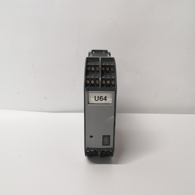
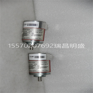


CMMTU02 用于自动化DCS监控数据传输模块
它的阴极连接到一个大的正偏压。在这种配置中,APD向运算放大器提供电流
使得输出相对于输入共模电压在负方向上摆动。到
OPA858共模被设置为接近正极限,
正极供电轨的电压为1.6 V。
反馈电阻RF和输入电容在噪声增益中形成一个零,如果留下会导致不稳定性
未经检查。为了抵消零的影响,通过将反馈电容器(CF.)添加到
噪声增益传递函数。高速放大器应用报告中的跨阻抗考虑
讨论说明如何补偿跨阻放大器特定增益的理论和方程
以及输入电容。应用程序报告中的带宽和补偿公式可在
Microsoft Excel™ 计算器关于跨阻抗放大器,您需要了解的内容–1部分提供了
链接到计算器。
光电二极管电容(pF)
闭环带宽,f-3dB(MHz)
集成输入参考噪声,I RN(nARMS)
反馈电阻(k:)
闭环带宽,f-3dB(MHz)
集成输入参考噪声,I RN(nARMS)
50 0
100 20
150 40
200 60
250 80
300 100
350 120
10 100
D210
f-3dB,CF=1 pF
f-3dB,CF=2 pF
IRN,CF=1 pF
IRN,CF=2 pF
21
OPA858
www.ti.com.SBOS629A–2018年4月–2018年7月修订
产品文件夹链接:OPA858
版权所有©2018,德克萨斯仪器公司提交文件反馈
申请资料(续)
图57.带宽和噪声性能与
光电二极管电容
图58.带宽和噪声性能与反馈
反对
上面引用的应用程序报告和博客文章中的等式和计算器用于建模
配置为TIA的OPA858的带宽(f-3dB)和噪声(IRN)性能。结果性能为:
如图57和图58所示。左侧Y轴显示闭环带宽性能,而
图的右侧显示了集成输入参考噪声。计算IRN的噪声带宽,对于固定
RF和CPD设置为等于f–3dB频率。
图57显示了在RF=10 kΩ和20
kΩ。增加CPD会降低闭环带宽。减少任何杂散寄生电容至关重要
PCB以大化带宽。OPA858的设计总输入电容为0.8 pF,以使
对系统性能的影响。
图58显示了CPD=1 pF和2 pF时放大器性能随射频的变化。增加射频导致
较低带宽。为了大化光学前端系统中的信噪比(SNR),大化增益
在TIA阶段。将射频增加一倍“X”会使信号电平增加“X”,但只会增加电阻
“噪声贡献”√从而提高SNR。
SBOS629A–2018年4月–2018年7月修订www.ti.com
产品文件夹链接:OPA858
提交文件反馈版权©2018,德克萨斯仪器公司
10.2典型应用
OPA858的高GBWP、低输入电压噪声和高转换速率使该器件成为可行的宽带、高性能和高性能的器件,
高输入阻抗电压放大器。
CMMTU02 用于自动化DCS监控数据传输模块

CMMTU02 用于自动化DCS监控数据传输模块
its cathode is tied to a large positive bias voltage. In this configuration the APD sources current into the op amp
feedback loop so that the output swings in a negative direction relative to the input common-mode voltage. To
maximize the output swing in the negative direction, the OPA858 common-mode is set close to the positive limit,
1.6 V from the positive supply rail.
The feedback resistance RF and the input capacitance form a zero in the noise gain that results in instability if left
unchecked. To counteract the effect of the zero, a pole is inserted by adding the feedback capacitor (CF.) into the
noise gain transfer function. The Transimpedance Considerations for High-Speed Amplifiers application report
discusses theories and equations that show how to compensate a transimpedance amplifier for a particular gain
and input capacitance. The bandwidth and compensation equations from the application report are available in a
Microsoft Excel ™ calculator. What You Need To Know About Transimpedance Amplifiers – Part 1 provides a
link to the calculator.
Photodiode capacitance (pF)
Closed-loop Bandwidth, f-3dB (MHz)
Integrated Input Referred Noise, I RN (nARMS)
Feedback Resistance (k:)
Closed-loop Bandwidth, f-3dB (MHz)
Integrated Input Referred Noise, I RN (nARMS)
50 0
100 20
150 40
200 60
250 80
300 100
350 120
10 100
D210
f-3dB, CF = 1 pF
f-3dB, CF = 2 pF
IRN, CF = 1 pF
IRN, CF = 2 pF
21
OPA858
www.ti.com SBOS629A –APRIL 2018–REVISED JULY 2018
Product Folder Links: OPA858
Copyright © 2018, Texas Instruments Incorporated Submit Documentation Feedback
Application Information (continued)
Figure 57. Bandwidth and Noise Performance vs
Photodiode Capacitance
Figure 58. Bandwidth and Noise Performance vs Feedback
Resistance
The equations and calculators in the application report and blog posts referenced above are used to model the
bandwidth (f-3dB) and noise (IRN) performance of the OPA858 configured as a TIA. The resultant performance is
shown in Figure 57 and Figure 58. The left side Y-axis shows the closed-loop bandwidth performance, while the
right side of the graph shows the integrated input referred noise. The noise bandwidth to calculate IRN, for a fixed
RF and CPD is set equal to the f–3dB frequency.
Figure 57 shows the amplifier performance as a function of photodiode capacitance (CPD) for RF = 10 kΩ and 20
kΩ. Increasing CPD decreases the closed-loop bandwidth. It is vital to reduce any stray parasitic capacitance from
the PCB to maximize bandwidth. The OPA858 is designed with 0.8 pF of total input capacitance to minimize the
effect on system performance.
Figure 58 shows the amplifier performance as a function of RF for CPD = 1 pF and 2 pF. Increasing RF results in
lower bandwidth. To maximize the signal-to-noise ratio (SNR) in an optical front-end system, maximize the gain
in the TIA stage. Increasing RF by a factor of "X" increases the signal level by "X", but only increases the resistor
noise contribution by "√X", thereby improving SNR.
SBOS629A –APRIL 2018–REVISED JULY 2018 www.ti.com
Product Folder Links: OPA858
Submit Documentation Feedback Copyright © 2018, Texas Instruments Incorporated
10.2 Typical Application
The high GBWP, low input voltage noise and high slew rate of the OPA858 makes the device a viable wideband,
high input impedance voltage amplifier.
Copyright ©2019-2022 瑞昌明盛自动化设备有限公司 版权所有 赣ICP备2021006016号