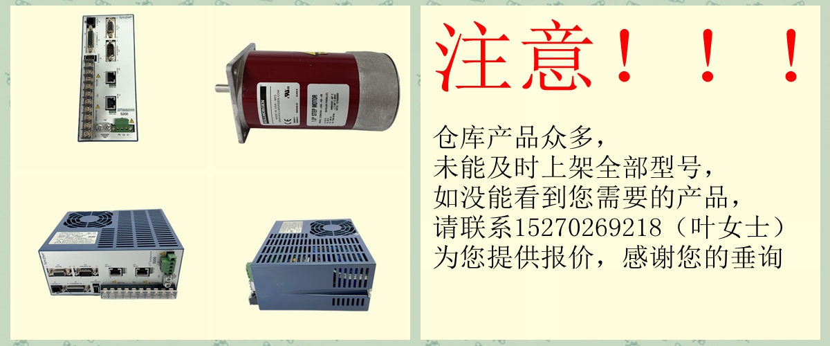


6205BZ10000K 125S2821-4 AA P195006 控制D/F主板用于驱动器
放大器的稳定性和相位裕度取决于放大器的环路增益,它是
放大器的AOL和反馈因子(β)。负反馈回路系统的β是
反馈到输入端的输出信号,在放大器的情况下,是噪声增益的倒数。这个
通过增加输入电容器和反馈,可以提高放大器在高频下的噪声增益
电容器如图60所示。如果小心操作,增加1/β可以改善相位裕度,就像任何放大器一样
与单位增益缓冲器配置相比,在高增益配置中更稳定。具有
增加的电容器改变高频噪声增益,但不改变信号增益。AN-1604
失补偿运算放大器应用报告提供了噪声增益整形的详细分析
失补偿放大器的技术,并展示如何选择外部电阻和电容值。
图61显示了如图59所示配置的OPA858的未补偿频率响应。
在没有任何附加噪声增益整形组件的情况下,OPA858显示约13dB的峰值。
图62显示了OPA858的噪声增益补偿频率响应,配置如所示
图60.噪声增益整形元件将峰值降低至小于1.5 dB。2.7pF输入电容器,
放大器的输入电容、增益电阻器和反馈电阻器在噪声增益中产生零
如等式2所示,频率为f。
哪里
•RF是反馈电阻器
•RG是输入或增益电阻器(包括源和终端电阻器的影响)
•CIN是总输入电容,包括外部2.7-pF电容器、放大器输入电容,
以及任何寄生PCB电容。(2)
等式2中的零增加了较高频率下的噪声增益,这在补偿
失补偿放大器。然而,噪声增益为零会降低环路增益相位,从而降低
相位裕度。为了抵消由于噪声增益为零而导致的相位降低,向噪声增益曲线添加极点
通过插入0.5pF反馈电容器。极点出现在等式3所示的频率处。噪声增益
必须选择极点和零点位置,以便AOL和
β约为20dB。为确保这一点,噪声增益极点必须出现在1/β幅值曲线之前
与AOL震级曲线相交。换句话说,噪声增益极点必须出现在|AOL|=| 1/β。要点
两条曲线相交的频率称为环路增益交叉频率。
哪里
•CF是反馈电容器(包括任何增加的PCB寄生)(3)
有关运算放大器稳定性的更多信息,请观看稳定性视频上的TI Precision Lab系列。
10.2.3应用曲线
VOUT=100 mVPP
图61.增益=–2 V/V,未补偿频率
回答
SBOS629A–2018年4月–2018年7月修订www.ti.com
产品文件夹链接:OPA858
提交文件反馈版权©2018,德克萨斯仪器公司
11电源建议
OPA858工作在3.3 V至5.25 V的电源上。OPA859工作在单面电源上,分体式
以及平衡双极性电源和不平衡双极电源。由于OPA858不具有轨道环形输入或输出,输入共模和输出摆动范围限制在3.3-V电源
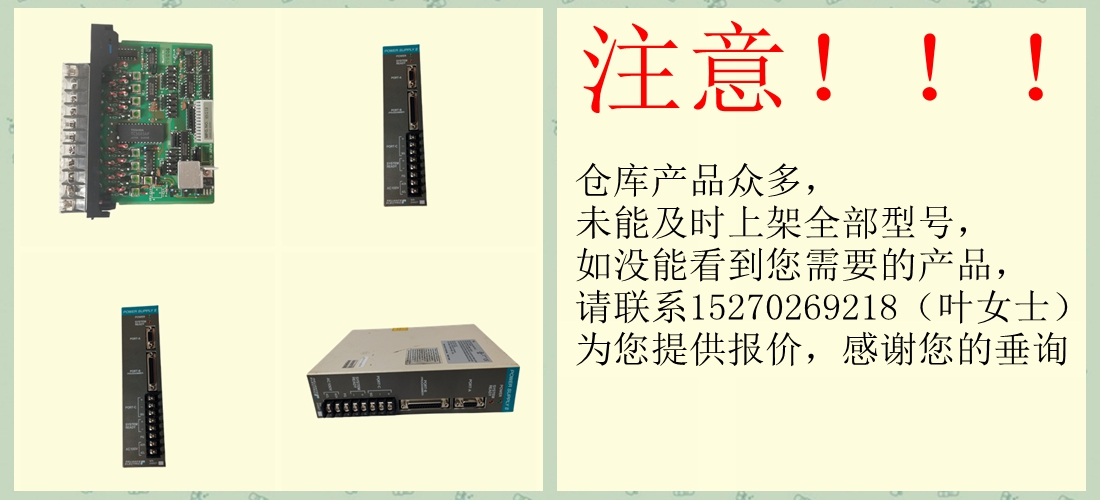
6205BZ10000K 125S2821-4 AA P195006 控制D/F主板用于驱动器

6205BZ10000K 125S2821-4 AA P195006 控制D/F主板用于驱动器
The stability and phase margin of the amplifier depend on the loop gain of the amplifier, which is the product of
the AOL and the feedback factor (β) of the amplifier. The β of a negative-feedback loop system is the portion of
the output signal that is fed back to the input, and in the case of an amplifier is the inverse of the noise gain. The
noise gain of the amplifier at high frequencies can be increased by adding an input capacitor and a feedback
capacitor as Figure 60 shows. If done carefully, increasing 1/β improves the phase margin just as any amplifier is
more stable in a high gain configuration versus a unity-gain buffer configuration. The modified network with the
added capacitors alters the high-frequency noise gain, but does not alter the signal gain. The AN-1604
Decompensated Operational Amplifiers application report provides a detailed analysis of noise gain-shaping
techniques for decompensated amplifiers and shows how to choose external resistors and capacitor values.
Figure 61 shows the uncompensated frequency response of the OPA858 configured as shown in Figure 59.
Without any added noise gain shaping components, the OPA858 shows approximately 13 dB of peaking.
Figure 62 shows the noise gain compensated frequency response of the OPA858 configured as shown in
Figure 60. The noise gain shaping elements reduce the peaking to less than 1.5 dB. The 2.7-pF input capacitor,
the input capacitance of the amplifier, the gain resistor, and the feedback resistor create a zero in the noise gain
at a frequency f, as Equation 2 shows.
where
• RF is the feedback resistor
• RG is the input or gain resistor (includes the effect of the source and termination resistor)
• CIN is the total input capacitance, which includes the external 2.7-pF capacitor, the amplifier input capacitance,
and any parasitic PCB capacitance. (2)
The zero in Equation 2 increases the noise gain at higher frequencies, which is important when compensating a
decompensated amplifier. However, the noise gain zero reduces the loop gain phase which results in a lower
phase margin. To counteract the phase reduction due to the noise gain zero, add a pole to the noise gain curve
by inserting the 0.5-pF feedback capacitor. The pole occurs at a frequency shown in Equation 3. The noise gain
pole and zero locations must be selected so that the rate-of-closure between the magnitude curves of AOL and
1/β is approximately 20 dB. To ensure this, the noise gain pole must occur before the 1/β magnitude curve
intersects the AOL magnitude curve. In other words, the noise gain pole must occur before |AOL| = |1/β|. The point
at which the two curves intersect is known as the loop gain crossover frequency.
where
• CF is the feedback capacitor (includes any added PCB parasitic) (3)
For more information on op amp stability, watch the TI Precision Lab series on stability video.
10.2.3 Application Curves
VOUT = 100 mVPP
Figure 61. Gain = –2 V/V, Uncompensated Frequency
Response
SBOS629A –APRIL 2018–REVISED JULY 2018 www.ti.com
Product Folder Links: OPA858
Submit Documentation Feedback Copyright © 2018, Texas Instruments Incorporated
11 Power Supply Recommendations
The OPA858 operates on supplies from 3.3 V to 5.25 V. The OPA858 operates on single-sided supplies, split
and balanced bipolar supplies, and unbalanced bipolar supplies. Because the OPA858 does not feature rail-torail inputs or outputs, the input common-mode and output swing ranges are limited at 3.3-V supplies
Copyright ©2019-2022 瑞昌明盛自动化设备有限公司 版权所有 赣ICP备2021006016号