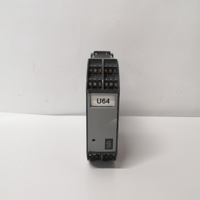


6205BZ10000B 125S2821-2 数字量D/F 板用于记录数据
等式2中的零增加了较高频率下的噪声增益,这在补偿
失补偿放大器。然而,噪声增益为零会降低环路增益相位,从而降低
相位裕度。为了抵消由于噪声增益为零而导致的相位降低,向噪声增益曲线添加极点
通过插入0.5pF反馈电容器。极点出现在等式3所示的频率处。噪声增益
必须选择极点和零点位置,以便AOL和
β约为20dB。为确保这一点,噪声增益极点必须出现在1/β幅值曲线之前
与AOL震级曲线相交。换句话说,噪声增益极点必须出现在|AOL|=| 1/β。要点
两条曲线相交的频率称为环路增益交叉频率。
哪里
•CF是反馈电容器(包括任何增加的PCB寄生)(3)
有关运算放大器稳定性的更多信息,请观看稳定性视频上的TI Precision Lab系列。
10.2.3应用曲线
VOUT=100 mVPP
图61.增益=–2 V/V,未补偿频率
回答
VOUT=100 mVPP
图62.增益=–2 V/V,补偿频率
回答
±
+
50-ü6RXUFH
六、
+
VS+
0.1ÖF
RT
49.9
RG
75
射频
453
6.8ÖF
b) 分流供电配置
a) 单电源配置
±
+
50-ü6RXUFH
六、
+
VS+
0.1ÖF
RT
49.9
RG
75
射频
453
6.8ÖF
200
+
0.1F 6.8F
VS±
200
VS+
2.
VS+
2.
VS+
2.
24
OPA858
SBOS629A–2018年4月–2018年7月修订www.ti.com
产品文件夹链接:OPA858
提交文件反馈版权©2018,德克萨斯仪器公司
11电源建议
OPA858工作在3.3 V至5.25 V的电源上。OPA859工作在单面电源上,分体式
以及平衡双极性电源和不平衡双极电源。由于OPA858不具有轨道环形输入或输出,输入共模和输出摆动范围限制在3.3-V电源。
图63.分体式和单电源电路配置
放置增益和反馈电阻器
接近引脚,大限度地减少杂散
电容
放置旁路电容器
靠近电源引脚
将散热垫连接到
负电源引脚
1 8
2 7
3 6
4 5
射频CBYP
RG RS
CBYP
热的
衬垫
将PD连接到VS+,以启用
放大器
NC(引脚2)隔离IN和FB
引脚,从而减少电容
耦合
接地和电源平面已拆除
从内层开始。地面填土
外层也被移除
地面和电源平面存在于
内层。
CBYP
RG射频
+
±
VSCBYP
VS+
典型示意图
RS
25
OPA858
www.ti.com.SBOS629A–2018年4月–2018年7月修订
产品文件夹链接:OPA858
版权所有©2018,德克萨斯仪器公司提交文件反馈
12布局
12.1布局指南
使用像OPA858这样的高频放大器实现佳性能需要仔细注意:
板布局寄生和外部组件类型。优化性能的建议包括:
1.小化从信号I/O引脚到交流接地的寄生电容。输出上的寄生电容
并且反相输入引脚可能导致不稳定性。为了减少不需要的电容,TI建议切断
信号输入和输出引脚下方的电源和接地迹线。否则,接地和电源
飞机必须在飞机上其他地方保持完好。将放大器配置为TIA时,如果需要
反馈电容器低于0.15 pF时,考虑使用两个串联电阻,每个电阻值为单个电阻值的一半
反馈回路中的电阻器,以小化电阻器的寄生电容。
2.尽量减少电源引脚与高频旁路电容器之间的距离(小于0.25英寸)
高质量、100 pF至0.1µF、C0G和NPO型去耦电容器,额定电压至少为三
大于放大器大电源的倍,以确保存在低阻抗路径
放大器电源引脚跨放大器增益带宽规格。在设备引脚处,执行
不允许接地和电源平面布局靠近信号I/O引脚。避窄
电源和接地迹线,以小化引脚和去耦电容器之间的电感。这个
电源连接必须始终与这些电容器去耦。更大(2.2-µF至6.8-µF)
在较低频率下有效的去耦电容器必须用于电源引脚。这些被放置
并且在PC板的同一区域中的多个设备之间共享
6205BZ10000B 125S2821-2 数字量D/F 板用于记录数据
6205BZ10000B 125S2821-2 数字量D/F 板用于记录数据
The zero in Equation 2 increases the noise gain at higher frequencies, which is important when compensating a
decompensated amplifier. However, the noise gain zero reduces the loop gain phase which results in a lower
phase margin. To counteract the phase reduction due to the noise gain zero, add a pole to the noise gain curve
by inserting the 0.5-pF feedback capacitor. The pole occurs at a frequency shown in Equation 3. The noise gain
pole and zero locations must be selected so that the rate-of-closure between the magnitude curves of AOL and
1/β is approximately 20 dB. To ensure this, the noise gain pole must occur before the 1/β magnitude curve
intersects the AOL magnitude curve. In other words, the noise gain pole must occur before |AOL| = |1/β|. The point
at which the two curves intersect is known as the loop gain crossover frequency.
where
• CF is the feedback capacitor (includes any added PCB parasitic) (3)
For more information on op amp stability, watch the TI Precision Lab series on stability video.
10.2.3 Application Curves
VOUT = 100 mVPP
Figure 61. Gain = –2 V/V, Uncompensated Frequency
Response
VOUT = 100 mVPP
Figure 62. Gain = –2 V/V, Compensated Frequency
Response
±
+
50-ü6RXUFH
VI
+
VS+
0.1 ÖF
RT
49.9
RG
75
RF
453
6.8 ÖF
b) Split supply configuration
a) Single supply configuration
±
+
50-ü6RXUFH
VI
+
VS+
0.1 ÖF
RT
49.9
RG
75
RF
453
6.8 ÖF
200
+
0.1 ÖF 6.8 ÖF
VS±
200
VS+
2
VS+
2
VS+
2
24
OPA858
SBOS629A –APRIL 2018–REVISED JULY 2018 www.ti.com
Product Folder Links: OPA858
Submit Documentation Feedback Copyright © 2018, Texas Instruments Incorporated
11 Power Supply Recommendations
The OPA858 operates on supplies from 3.3 V to 5.25 V. The OPA858 operates on single-sided supplies, split
and balanced bipolar supplies, and unbalanced bipolar supplies. Because the OPA858 does not feature rail-torail inputs or outputs, the input common-mode and output swing ranges are limited at 3.3-V supplies.
Figure 63. Split and Single Supply Circuit Configuration
Place gain and feedback resistors
close to pins to minimize stray
capacitance
Place bypass capacitor
close to power pins
Connect the thermal pad to the
negative supply pin
1 8
2 7
3 6
4 5
RF CBYP
RG RS
CBYP
Thermal
Pad
Connect PD to VS+ to enable the
amplifier
NC (Pin 2) isolates the IN- and FB
pins thereby reducing capacitive
coupling
Ground and power plane removed
from inner layers. Ground fill on
outer layers also removed
Ground and power plane exist on
inner layers.
CBYP
RG RF
+
±
VSCBYP
VS+
Representative schematic
RS
25
OPA858
www.ti.com SBOS629A –APRIL 2018–REVISED JULY 2018
Product Folder Links: OPA858
Copyright © 2018, Texas Instruments Incorporated Submit Documentation Feedback
12 Layout
12.1 Layout Guidelines
Achieving optimum performance with a high-frequency amplifier like the OPA858 requires careful attention to
board layout parasitics and external component types. Recommendations that optimize performance include:
1. Minimize parasitic capacitance from the signal I/O pins to AC ground. Parasitic capacitance on the output
and inverting input pins can cause instability. To reduce unwanted capacitance, TI recommends cutting out
the power and ground traces underneath the signal input and output pins. Otherwise, ground and power
planes must be unbroken elsewhere on the board. When configuring the amplifier as a TIA, if the required
feedback capacitor is under 0.15 pF, consider using two series resistors, each of half the value of a single
resistor in the feedback loop to minimize the parasitic capacitance from the resistor.
2. Minimize the distance (less than 0.25") from the power-supply pins to high-frequency bypass capacitors. Use
high quality, 100-pF to 0.1-µF, C0G and NPO-type decoupling capacitors with voltage ratings at least three
times greater than the amplifiers maximum power supplies to ensure that there is a low-impedance path to
the amplifiers power-supply pins across the amplifiers gain bandwidth specification. At the device pins, do
not allow the ground and power plane layout to be in close proximity to the signal I/O pins. Avoid narrow
power and ground traces to minimize inductance between the pins and the decoupling capacitors. The
power-supply connections must always be decoupled with these capacitors. Larger (2.2-µF to 6.8-µF)
decoupling capacitors, effective at lower frequency, must be used on the supply pins. These are placed
further from the device and are shared among several devices in the same area of the PC board
Copyright ©2019-2022 瑞昌明盛自动化设备有限公司 版权所有 赣ICP备2021006016号