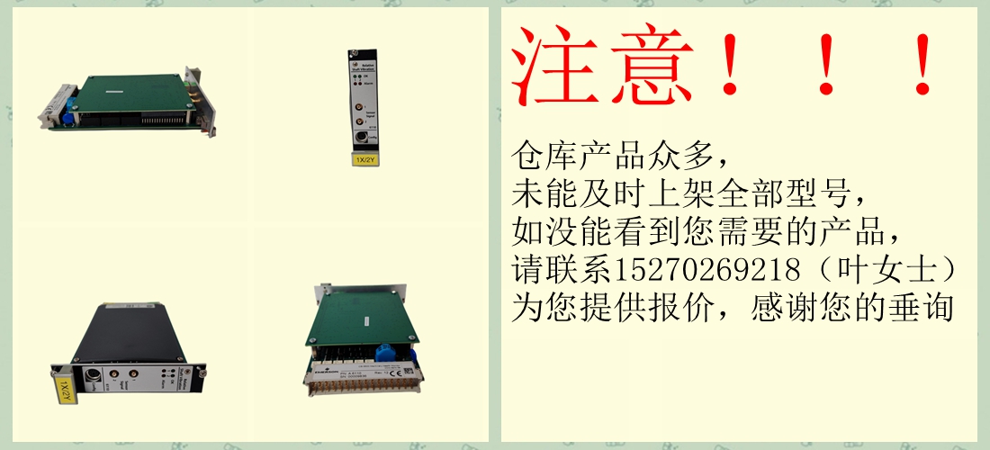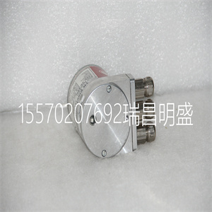


6205BZ10000G 125S2821-2 伺服主控制D/F 板用于自能驱动
1.布局指南
使用像OPA858这样的高频放大器实现佳性能需要仔细注意:
板布局寄生和外部组件类型。优化性能的建议包括:
1.小化从信号I/O引脚到交流接地的寄生电容。输出上的寄生电容
并且反相输入引脚可能导致不稳定性。为了减少不需要的电容,TI建议切断
信号输入和输出引脚下方的电源和接地迹线。否则,接地和电源
飞机必须在飞机上其他地方保持完好。将放大器配置为TIA时,如果需要
反馈电容器低于0.15 pF时,考虑使用两个串联电阻,每个电阻值为单个电阻值的一半
反馈回路中的电阻器,以小化电阻器的寄生电容。
2.尽量减少电源引脚与高频旁路电容器之间的距离(小于0.25英寸)
高质量、100 pF至0.1µF、C0G和NPO型去耦电容器,额定电压至少为三
大于放大器大电源的倍,以确保存在低阻抗路径
放大器电源引脚跨放大器增益带宽规格。在设备引脚处,执行
不允许接地和电源平面布局靠近信号I/O引脚。避窄
电源和接地迹线,以小化引脚和去耦电容器之间的电感。这个
电源连接必须始终与这些电容器去耦。更大(2.2-µF至6.8-µF)
在较低频率下有效的去耦电容器必须用于电源引脚。这些被放置
并且在PC板的相同区域中的多个设备之间共享。
3.仔细选择和放置外部组件,以保持高频性能
使用低电抗电阻器。表面贴装电阻器工作佳,整体更紧密
布局切勿在高频应用中使用线绕电阻器。因为输出引脚和反相
输入引脚对寄生电容敏感,始终定位反馈和串联输出
电阻器(如有)尽可能靠近输出引脚。放置其他网络组件(如非反相
输入端接电阻器)。即使在低寄生电容分流外部
电阻器,高电阻值会产生显著的时间常数,从而降低性能。什么时候
将OPA858配置为电压放大器,使电阻值尽可能低并与
负载驱动注意事项。减小电阻器值可保持电阻器噪声项较低,并将其小化
寄生电容的影响。然而,较低的电阻值会增加动态功率
因为RF和RG成为放大器输出负载网络的一部分。
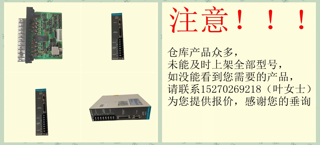
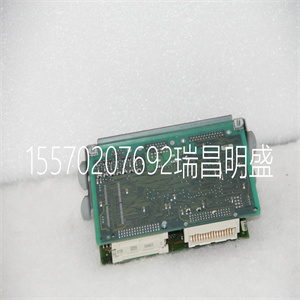
6205BZ10000G 125S2821-2 伺服主控制D/F 板用于自能驱动
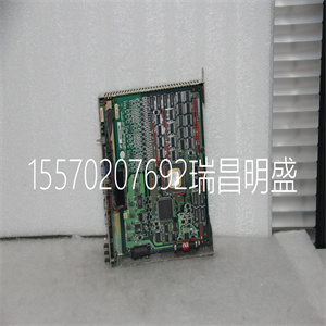
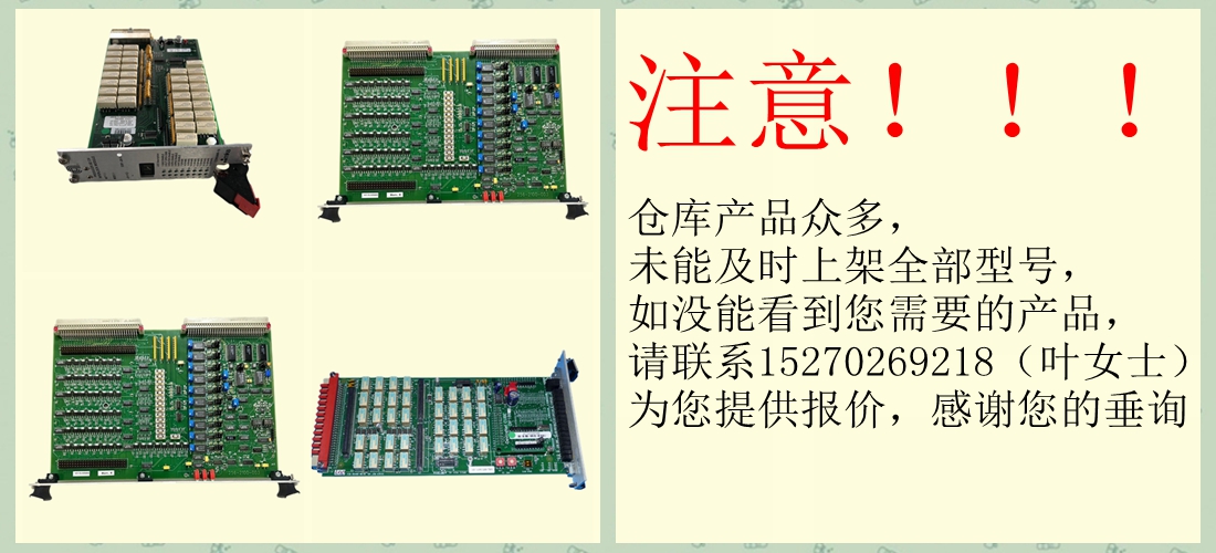
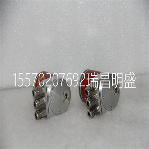
6205BZ10000G 125S2821-2 伺服主控制D/F 板用于自能驱动
1 Layout Guidelines
Achieving optimum performance with a high-frequency amplifier like the OPA858 requires careful attention to
board layout parasitics and external component types. Recommendations that optimize performance include:
1. Minimize parasitic capacitance from the signal I/O pins to AC ground. Parasitic capacitance on the output
and inverting input pins can cause instability. To reduce unwanted capacitance, TI recommends cutting out
the power and ground traces underneath the signal input and output pins. Otherwise, ground and power
planes must be unbroken elsewhere on the board. When configuring the amplifier as a TIA, if the required
feedback capacitor is under 0.15 pF, consider using two series resistors, each of half the value of a single
resistor in the feedback loop to minimize the parasitic capacitance from the resistor.
2. Minimize the distance (less than 0.25") from the power-supply pins to high-frequency bypass capacitors. Use
high quality, 100-pF to 0.1-µF, C0G and NPO-type decoupling capacitors with voltage ratings at least three
times greater than the amplifiers maximum power supplies to ensure that there is a low-impedance path to
the amplifiers power-supply pins across the amplifiers gain bandwidth specification. At the device pins, do
not allow the ground and power plane layout to be in close proximity to the signal I/O pins. Avoid narrow
power and ground traces to minimize inductance between the pins and the decoupling capacitors. The
power-supply connections must always be decoupled with these capacitors. Larger (2.2-µF to 6.8-µF)
decoupling capacitors, effective at lower frequency, must be used on the supply pins. These are placed
further from the device and are shared among several devices in the same area of the PC board.
3. Careful selection and placement of external components preserves the high-frequency performance
of the OPA858 . Use low-reactance resistors. Surface-mount resistors work best and allow a tighter overall
layout. Never use wirewound resistors in a high-frequency application. Because the output pin and inverting
input pin are the most sensitive to parasitic capacitance, always position the feedback and series output
resistor, if any, as close to the output pin as possible. Place other network components (such as noninverting
input termination resistors) close to the package. Even with a low parasitic capacitance shunting the external
resistors, high resistor values create significant time constants that can degrade performance. When
configuring the OPA858 as a voltage amplifier, keep resistor values as low as possible and consistent with
load driving considerations. Decreasing the resistor values keeps the resistor noise terms low and minimizes
the effect of the parasitic capacitance. However, lower resistor values increase the dynamic power
consumption because RF and RG become part of the output load network of the amplifier.
Copyright ©2019-2022 瑞昌明盛自动化设备有限公司 版权所有 赣ICP备2021006016号